Tda8954
Содержание:
TDA8954TH Datasheet PDF — NXP
| Part Number | TDA8954TH | |
| Description | 2 X 210 W class-D power amplifier | |
| Manufacturers | NXP | |
| Logo | ||
Preview ( 30 pages )
TDA8954

2 × 210 W class-D power amplifier

Rev. 01 — 24 December 2009
Product data sheet
1. General description
The TDA8954 is a stereo or mono high-efficiency Class D audio power amplifier in a

single IC featuring low power dissipation. It is designed to deliver up to 2 × 210 W into a


4 Ω load in a stereo Single-Ended (SE) application, or 1 × 420 W into an 8 Ω load in a

mono Bridge-Tied Load (BTL) application.

It combines the benefits of Class D efficiency (≈93 % into a 4 Ω load) with audiophile

sound quality comparable to that associated with Class AB amplification.

The amplifier operates over a wide supply voltage range from ±12.5 V to ±42.5 V and

features low quiescent current consumption.
The TDA8954 is supplied with two diagnostic pins for monitoring the status of Thermal
Fold Back (TFB), Over Current Protection (OCP) and other protection circuits.
2. Features

High output power in typical applications:


SE 2 × 210 W, RL = 4 Ω (VDD = 41 V; VSS = −41 V)


SE 2 × 235 W, RL = 3 Ω (VDD = 39 V; VSS = −39 V)


SE 2 × 150 W, R = 6 Ω (V = 41 V; V = −41 V)www.DataSheet.net/

L DD
SS

BTL 1 × 420 W, RL = 8 Ω (VDD = 41 V; VSS = −41 V)


Symmetrical operating supply voltage range from ±12.5 V to ±42.5 V


Stereo full differential inputs, can be used as stereo SE or mono BTL amplifier


Low noise


Smooth pop noise-free start-up and switch off


2-pin diagnostics for protection circuits


Fixed frequency internal or external clock


High efficiency ≈93 %


Zero dead time switching


Low quiescent current


Advanced protection strategy: voltage protection and output current limiting


Thermal FoldBack (TFB) with disable functionality


Fixed gain of 30 dB in SE and 36 dB in BTL applications


Fully short-circuit proof across load


BD modulation in BTL configuration


Clock protection

Datasheet pdf - http://www.DataSheet4U.co.kr/
1 page 2 × 210 W class-D power amplifier 7.2 Pin description (PWM) signal using an analog input stage and a PWM modulator; see Figure 1. To drive the output power transistors, the digital PWM signal is fed to a control and handshake |
||
| Information | Total 30 Pages | |
| Download |
 NXP Semiconductors
Share Link :
Electronic Components Distributor
| SparkFun Electronics | Allied Electronics | DigiKey Electronics | Arrow Electronics |
| Mouser Electronics | Adafruit | Element14 | Chip One Stop |
Featured Datasheets
| Part Number | Description | Manufacturers |
| TDA8954TH | The function is 2 X 210 W class-D power amplifier. | NXP |
|
Quick jump to:
TDA8 |
TDA8954J Datasheet Download — NXP
| Номер произв | TDA8954J | |||
| Описание | 2 X 210 W class-D power amplifier | |||
| Производители | NXP | |||
| логотип | ||||
1Page
TDA8954 2 × 210 W class-D power amplifier Rev. 01 — 24 December 2009 single IC featuring low power dissipation. It is designed to deliver up to 2 × 210 W into a 4 Ω load in a stereo Single-Ended (SE) application, or 1 × 420 W into an 8 Ω load in a mono Bridge-Tied Load (BTL) application. It combines the benefits of Class D efficiency (≈93 % into a 4 Ω load) with audiophile sound quality comparable to that associated with Class AB amplification. The amplifier operates over a wide supply voltage range from ±12.5 V to ±42.5 V and features low quiescent current consumption. High output power in typical applications: SE 2 × 210 W, RL = 4 Ω (VDD = 41 V; VSS = −41 V) SE 2 × 235 W, RL = 3 Ω (VDD = 39 V; VSS = −39 V) SE 2 × 150 W, R = 6 Ω (V = 41 V; V = −41 V)www.DataSheet.net/ L DD BTL 1 × 420 W, RL = 8 Ω (VDD = 41 V; VSS = −41 V) Symmetrical operating supply voltage range from ±12.5 V to ±42.5 V Stereo full differential inputs, can be used as stereo SE or mono BTL amplifier Low noise Smooth pop noise-free start-up and switch off 2-pin diagnostics for protection circuits Fixed frequency internal or external clock High efficiency ≈93 % Zero dead time switching Low quiescent current Advanced protection strategy: voltage protection and output current limiting Thermal FoldBack (TFB) with disable functionality Fixed gain of 30 dB in SE and 36 dB in BTL applications Fully short-circuit proof across load BD modulation in BTL configuration Clock protection Datasheet pdf — http://www.DataSheet4U.co.kr/
NXP Semiconductors 2 × 210 W class-D power amplifier 3. Applications DVD Mini and micro receiver Subwoofers Home Theater In A Box (HTIAB) system High-power speaker system Public Address (PA) system 4. Quick reference data VDD VSS Vth(ovp) positive supply voltage Standby, Mute modes; VDD − VSS IDD(tot) total positive supply current the sum of the currents through pins VDDA, VDDP1 and VDDP2 ISS(tot) total negative supply current the sum of the currents through pins VSSA, VSSP1 and VSSP2 Po output power Tj = 85 °C; LLC = 15 μH; CLC = 680 nF (see Figure 13) THD + N = 10 %; RL = 4 Ω; VDD = 41 V; VSS = −41 V THD + N = 10 %; RL = 4 Ω; VDD = 35 V; VSS = −35 V Po output power Tj = 85 °C; LLC = 22 μH; CLC = 680 nF (see Figure 13); RL = 8 Ω; THD + N = 10 %; VDD = 41 V; VSS = −41 V Min Typ 12.5 41 −12.5 −41 85 — — — — 420 −42.5 V 90 V VDD is the supply voltage on pins VDDP1, VDDP2 and VDDA. VSS is the supply voltage on pins VSSP1, VSSP2 and VSSA. Output power is measured indirectly; based on RDSon measurement; see Section 14.3. 5. Ordering information
NXP Semiconductors 2 × 210 W class-D power amplifier VDDA DIAG1 11 (5) mute 7 (1) SWITCH1 CONTROL AND |
||||
| Всего страниц | 30 Pages | |||
| Скачать PDF |

TDA8950J
The TDA8950 is a high-efficiency Class D 2-channel audio power amplifier chip. The typical power output is 150Watts per channel with a speaker load impedance of 4 Ω. The TDA8950 chip operates over a wide supply voltage range from ±12.5 V to ±40 V and features low quiescent current consumption.
Features of TDA8950:
- Symmetrical operating supply voltage range from ±12.5 V to ±40 V
- Stereo full differential inputs, can be used as stereo Single-Ended (SE) or mono Bridge-Tied Load (BTL) amplifier
- High output power in typical applications: SE 2 × 150 W, R L = 4 Ω (V P = ±37 V) SE 2 × 170 W, R L = 4 Ω (V P = ±39 V) SE 2 × 100 W, R L = 6 Ω (V P = ±37 V) BTL 1 × 300 W, R L = 8 Ω (V P = ±37 V)
- Low noise
- Smooth pop noise-free start-up and switch off
- Zero dead time switching
- High efficiency
- Low quiescent current
- Advanced protection strategy: voltage protection and output current limiting
- Thermal FoldBack (TFB)Fixed gain of 30 dB in SE and 36 dB in BTL applications
- Fully short-circuit proof across load
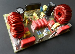
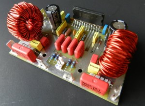
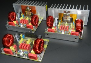
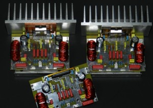
For this project the TDA8950 is configured as a mono Full Bridge Class D power amplifier. This configuration was chosen to effectively avoid a strange phenomenon of a typical Class D power amplifiers called «pumping effect».
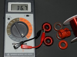
The tricky part of building this project is the toroidal-cored low pass filter inductors, L1 and L2. The inductor is made up of 75” of 18AWG enameled copper wire wound on a T106-2 core. After winding the coil, verify the inductance with an LCR meter, it should read about 37uH. With this value the idle current of the amplifier is about 48 to 50mA. The original NXP Semiconductors’ schematic diagram of this project as well as other information about TDA8950 are found here: TDA8950 datasheet. However, if you’re interested in building this project and have read the Information and Policies section of this website, the schematic diagram, PCB layout (available only by request) and BOM are free, as is, no warranty. Enjoy!
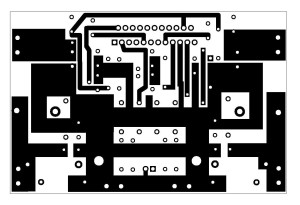
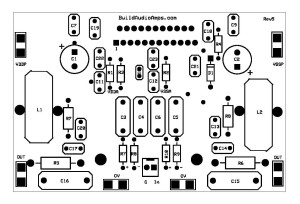
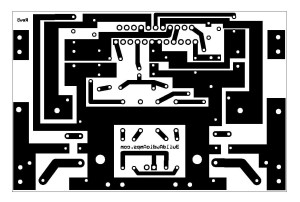
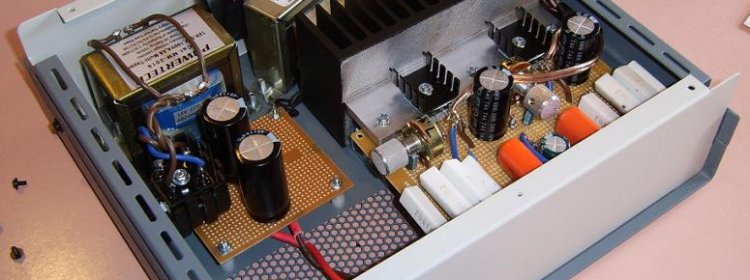
TDA8950J Top Layer TDA8950J Silkscreen Parts Placement Layer TDA8950J Bottom Copper Layer
Updated 12-22-2014
Cut the copper trace that runs from pin2 of J1 to the main ground (see top layer of PCB). Solder a piece of hook-up wire from pin2 of J1 to pin19 of TDA8950 (see picture below). This will eliminate the high-pitched noise caused by signal/power grounding problem and improves overall sound quality. When testing the project without a pre-amp it is necessary to install a shunt or jumper at J1, also shown in picture below. The update is not needed when the project is powered at ±25VDC rails.


Связанные материалы
Аудиосистема класса Hi-Fi своими руками: советы и секреты. Андреев Д. А., Торопкин М. В….
Андреев Д. А., Торопкин М. В., Аудиосистема класса Hi-Fi своими руками: советы и секреты. -СПб.:…
 Однотактный усилитель Хьюстона класса А на 2SK1058 MOSFET-е. ZCA — усилитель без деталей…
Mark Houston and diyAudioProjects.com Igor «Datagor» Kotov — авторский перевод Мне захотелось…
 Усилитель 2.1 для портативного плеера. Чип MAX98400 — мощный усилитель класса D в действии…
Компания MAXIM представила 11 ноября 2011 г. обновленный Reference Design #4320В, который включает…
Колонки DMT-100 по Driver Manipulation Technology. Удивительное рядом…
Расскажу я вам, ребяты, как аллюминиевые штанги и стекловолоконные шары скрутить вместе и продать…
Выбираем правильный разъем Jack для гитары. Легкий моддинг углового штекера Neutrik NP2R…
Собственно, к угловому штекеру «Neutrik NP2R» у меня больших претензий нет. Впервые приобретя…
 Пассивные колонки из того, что было под рукой, на 6ГД-6 для компьютера…
Были у меня старенькие динамики 6ГД-6, вот решил сделать из них колонки к компьютеру взамен дешёвых…
Напольные трехполосные АС…
Идея собрать АС родилась давно, но не было то времени, то возможности. Наконец собравшись, решил,…
Усилитель «The Naked Amp» на 3-х транзисторах…
Этот усилитель я собрал 4 месяца назад на работе из того, что было под рукой. Название усилителя…
Определение ёмкости конденсатора по цифровой маркировке из трёх знаков…
Цифровая маркировка используется уже довольно давно. На малогабаритных конденсаторах чаще всего она…
 Доработка штатной аудиосистемы Nissan Primera P12…
Всем привет. Я очень давно увлекаюсь автозвуком и все мои машины были очень хорошо упакованы…
Акустическая система с лабиринтом 35ГДН–4 + 2ГД36…
Недорогая акустическая система на доступных динамиках с лабиринтом, обладающая хорошим качеством…
Усилитель на MAX9768. Способна ли ЛУТ подковать «блоху» класса D?…
Решили мы с приятелем сделать бумбокс — очень уж понравилась работа финских парней, да и идея давно…
Камрад, рассмотри датагорские рекомендации
Внимание! 800 рублей для новичков на Aliexpress Регистрируйтесь по нашей ссылке. Если вы впервые на Aliexpress — получите 800.00₽ купонами на свой первый заказ.. Цифровой осциллограф DSO138
Кит для сборки
Цифровой осциллограф DSO138. Кит для сборки
Функциональный генератор. Кит для сборки
Настраиваемый держатель для удобной пайки печатных плат
Владимир Мосягин (MVV)
Россия, Великий Новгород
Список всех статей
Профиль MVV
Радиолюбительством увлекся с пятого класса средней школы.Специальность по диплому — радиоинженер, к.т.н.Автор книг «Юному радиолюбителю для прочтения с паяльником», «Секреты радиолюбительского мастерства», соавтор серии книг «Для прочтения с паяльником» в издательстве «СОЛОН-Пресс», имею публикации в журналах «Радио», «Приборы и техника эксперимента» и др.