Даташит stv9302a pdf ( datasheet )
STV9326 Datasheet Download — ST Microelectronics
| Номер произв | STV9326 | |||
| Описание | Vertical Deflection Booster | |||
| Производители | ST Microelectronics | |||
| логотип | ||||
1Page
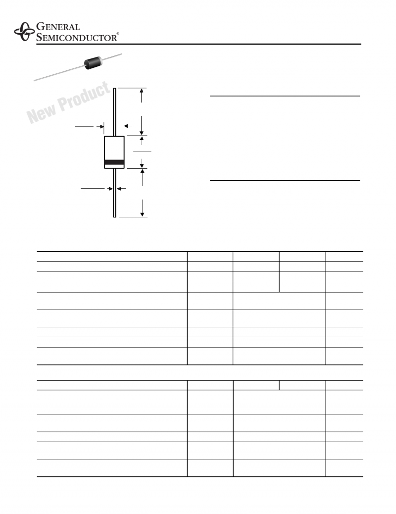
www.DataSheet4U.com STV9326 Vertical Deflection Booster for 3-APPTV/Monitor Applications with 60-V Flyback Generator Main Features ■ Power Amplifier ■ Flyback Generator ■ Stand-by Control ■ Output Current up to 3 App ■ Thermal Protection HEPTAWATT DataSheet4U.com to pin 4 In double-supply applications, a stand-by state will Non-Inverting 7 Input Input 1 + 5 Output DataSheet4U.com DataSheet4 U .com Revision 1.1
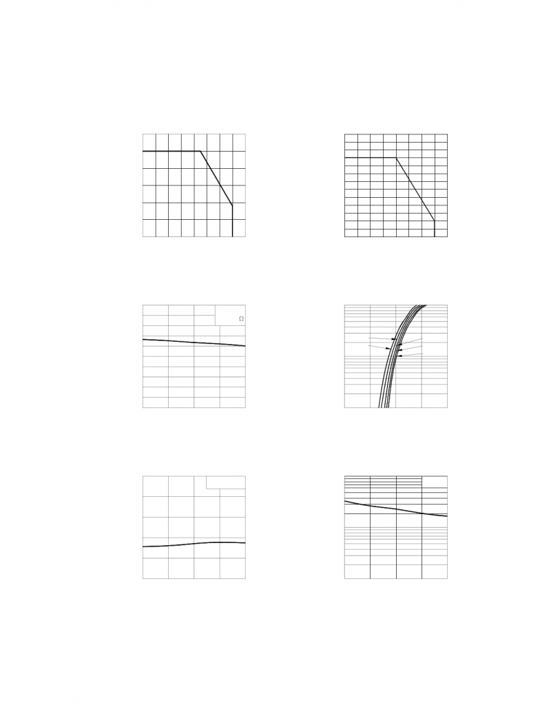
www.DataSheet4U.com VS Supply Voltage (pin 2) — Note 1 and Note 2 V5, V6 Flyback Peak Voltage — Note 2 V3 Voltage at Pin 3 — Note 2, Note 3 and Note 6 V1, V7 Amplifier Input Voltage — Note 2, Note 6 and Note 7 Current I(1) Output Peak Current at f = 50 to 200 Hz, t ≤ 10µs — Note 4 I(2) Output Peak Current non-repetitive — Note 5 I3 Sink Sink Current, t<1ms — Note 3 I3 Source Source Current, t < 1ms I3 Flyback pulse current at f=50 to 200 Hz, t≤10µs — Note 4 ESD Susceptibility Human body model (100 pF discharged through 1.5 kΩ) ESD2 EIAJ Standard (200 pF discharged through 0 Ω) Temperature Ts Tj Storage Temperature -0.4 to (VS + 3) — 0.4 to (VS + 2) or +40 V °C DataShee Note:1. Usually the flyback voltage is slightly more than 2 x VS. This must be taken into consideration when setting VS. 2. Versus pin 4 3. V3 is higher than VS during the first half of the flyback pulse. 4. Such repetitive output peak currents are usually observed just before and after the flyback pulse. Off phases. This peak current is acceptable providing the SOA is respected (Figure 8 and Figure 9). 6. All pins have a reverse diode towards pin 4, these diodes should never be forward-biased. 7. Input voltages must not exceed the lower value of either VS + 2 or 40 volts. 2 Thermal Data RthJC TT TJ DataSheet4U.com DataSheet4 U .com Parameter
www.DataSheet4U.com (VS = 29 V, TAMB = 25°C, unless otherwise specified) Symbol VS Operating Supply Voltage Range (V2-V4) Note 8 I2 Pin 2 Quiescent Current I3 = 0, I5 = 0 I6 Pin 6 Quiescent Current I3 = 0, I5 = 0, V6 =30v Input I1 Input Bias Current V1 = 1 V, V7 = 2.2 V I7 Input Bias Current V1 = 2.2 V, V7 = 1 V VIR Operating Input Voltage Range VI0 Offset Voltage ∆VI0/dt Offset Drift versus Temperature Output IOperating Peak Output Current o<Tcase<125oC V5L Output Saturation Voltage to pin 4 I5 = 1.5 A V5H Output Saturation Voltage to pin 6 I5 = -1.5 A et4U.comStand-by V5STBY Output Voltage in Stand-by DataSheet4U.com V1 = V7 = VS = 0 See Note 9 Miscellaneous VD5-6 Diode Forward Voltage Between pins 5-6 I5 = 1.5 A VD3-2 Diode Forward Voltage between pins 3-2 I3 = 1.5 A V3SL Saturation Voltage on pin 3 I3 = 20 mA V3SH Saturation Voltage to pin 2 (2nd part of flyback) I3 = -1.5 A Min. Typ. Max. Unit Fig. — 0.6 -1.5 µA 1 — 0.6 -1.5 µA 0 VS — 2 V 2 mV 10 µV/°C ±1.5 1 1.7 VS — 2 V 8. In normal applications, the peak flyback voltage is slightly greater than 2 x (VS — V4). Therefore, (VS — V4) = 30 V is not allowed without special circuitry. 9. Refer to Figure 4, Stand-by condition. DataSheet4U.com DataSheet4 U .com 3/14 |
||||
| Всего страниц | 14 Pages | |||
| Скачать PDF |


