4468
Содержание:
- 2STC4468 Datasheet (PDF)
- 2STW4468 Datasheet (PDF)
- AO4468 Datasheet (PDF)
- Биполярный транзистор 2STC4468 — описание производителя. Основные параметры. Даташиты.
- 2STC4468 Datasheet (PDF)
- AO4916 MOSFET — описание производителя. Даташиты. Основные параметры и характеристики. Поиск аналога. Справочник
- AO4916 Datasheet (PDF)
- Биполярный транзистор 2SC4468 — описание производителя. Основные параметры. Даташиты.
- 2SC4468 Datasheet (PDF)
- IRFP4468 Datasheet (PDF)
- AON6992 MOSFET — описание производителя. Даташиты. Основные параметры и характеристики. Поиск аналога. Справочник
- AON6992 Datasheet (PDF)
- AON6406 Datasheet (PDF)
- FDS4465 Datasheet (PDF)
- AO4916 Datasheet (PDF)
- AO4468 MOSFET — описание производителя. Даташиты. Основные параметры и характеристики. Поиск аналога. Справочник
- AO4468 Datasheet (PDF)
- FDS4685 MOSFET — описание производителя. Даташиты. Основные параметры и характеристики. Поиск аналога. Справочник
- FDS4685 Datasheet (PDF)
- Биполярный транзистор 2SC4407 — описание производителя. Основные параметры. Даташиты.
- 2SC4407 Datasheet (PDF)
- AO4478 MOSFET — описание производителя. Даташиты. Основные параметры и характеристики. Поиск аналога. Справочник
- AO4478 Datasheet (PDF)
2STC4468 Datasheet (PDF)
1.1. 2stc4468.pdf Size:165K _st
2STC4468
High power NPN epitaxial planar bipolar transistor
Features
High breakdown voltage VCEO = 140 V
Complementary to 2STA1695
Typical ft = 20 MHz
Fully characterized at 125 oC
3
Application
2
1
Audio power amplifier
TO-3P
Description
Figure 1. Internal schematic diagram
The device is a NPN transistor manufactured
using new BiT-LA (Bipolar transistor for linear
amp
3.1. 2stc4467.pdf Size:143K _st
2STC4467
High power NPN epitaxial planar bipolar transistor
Features
High breakdown voltage VCEO = 120 V
Complementary to 2STA1694
Fast-switching speed
Typical ft = 20 MHz
Fully characterized at 125 oC
3
2
1
Applications
TO-3P
Audio power amplifier
Description
Figure 1. Internal schematic diagram
The device is a NPN transistor manufactured
using new BiT-LA (Bipolar tr
5.1. 2stc4793.pdf Size:136K _st
2STC4793
NPN power bipolar transistor
Preliminary data
Features
High breakdown voltage VCEO = 230 V
Complementary to 2STA1837
High transition frequency, typical fT = 100 MHz
Applications
Audio power amplifier
3
2
Drive stage amplifier
1
TO-220FP
Description
This device is a NPN transistor manufactured
using new PB-HDC (power bipolar high density
Figure 1. Internal sc
2STW4468 Datasheet (PDF)
1.1. 2stw4468.pdf Size:161K _st
2STW4468
High power NPN epitaxial planar bipolar transistor
Features
High breakdown voltage VCEO = 140 V
Complementary to 2STW1695
Fast-switching speed
Typical ft = 20 MHz
Fully characterized at 125 oC
3
2
1
Applications
TO-247
Audio power amplifier
Description
Figure 1. Internal schematic diagram
The device is a NPN transistor manufactured
using new BiT-LA (Bipolar t
3.1. 2stw4466.pdf Size:162K _st
2STW4466
High power NPN epitaxial planar bipolar transistor
Features
High breakdown voltage VCEO = 80 V
Complementary to 2STW1693
Typical ft = 20 MHz
Fully characterized at 125 oC
Applications
3
2
Audio power amplifier
1
TO-247
Description
The device is a NPN transistor manufactured in
Figure 1. Internal schematic diagram
low voltage planar technology using base island
AO4468 Datasheet (PDF)
1.1. ao4468.pdf Size:315K _aosemi


AO4468
30V N-Channel MOSFET
General Description Product Summary
VDS
30V
The AO4468 combines advanced trench MOSFET
technology with a low resistance package to provide
ID (at VGS=10V) 10.5A
extremely low RDS(ON). This device is ideal for load switch
RDS(ON) (at VGS=10V) 1.2. ao4468.pdf Size:1303K _kexin


SMD Type MOSFET
N-Channel MOSFET
AO4468 (KO4468)
SOP-8
■ Features
● VDS (V) = 30V
1.50 0.15
● ID = 10.5 A (VGS = 10V)
● RDS(ON) < 17mΩ (VGS = 10V)
1 Source 5 Drain
● RDS(ON) < 23mΩ (VGS = 4.5V)
6 Drain
2 Source
7 Drain
3 Source
8 Drain
4 Gate
D
G
S
■ Absolute Maximum Ratings Ta = 25℃
Parameter Symbol Rating Unit
Drain-Source Voltage VDS 30
V
Gat
5.1. ao4466l.pdf Size:199K _update-mosfet
AO4466
N-Channel Enhancement Mode Field Effect Transistor
General Description Features
The AO4466/L uses advanced trench technology to VDS (V) = 30V
provide excellent RDS(ON) and low gate charge. This
ID = 9.4A (VGS = 10V)
device is suitable for use as a load switch or in PWM
RDS(ON) 5.2. ao4466.pdf Size:324K _aosemi


AO4466
30V N-Channel MOSFET
General Description Product Summary
The AO4466 uses advanced trench technology to VDS (V) = 30V
provide excellent RDS(ON) and low gate charge. This ID = 10A (VGS = 10V)
device is suitable for use as a load switch or in PWM
RDS(ON)
5.3. ao4466l.pdf Size:199K _aosemi


AO4466
N-Channel Enhancement Mode Field Effect Transistor
General Description Features
The AO4466/L uses advanced trench technology to VDS (V) = 30V
provide excellent RDS(ON) and low gate charge. This
ID = 9.4A (VGS = 10V)
device is suitable for use as a load switch or in PWM
RDS(ON) 5.4. ao4466.pdf Size:1389K _kexin
SMD Type MOSFET
N-Channel MOSFET
AO4466 (KO4466)
SOP-8
■ Features
● VDS (V) = 30V
● ID = 9.4 A (VGS = 10V)
1.50 0.15
● RDS(ON) < 23mΩ (VGS = 10V)
● RDS(ON) < 35mΩ (VGS = 4.5V)
1 Source 5 Drain
6 Drain
2 Source
7 Drain
3 Source
8 Drain
4 Gate
D
G
S
■ Absolute Maximum Ratings Ta = 25℃
Parameter Symbol Rating Unit
Drain-Source Voltage VDS 30
V
Gate
Биполярный транзистор 2STC4468 — описание производителя. Основные параметры. Даташиты.
Наименование производителя: 2STC4468
Тип материала: Si
Полярность: NPN
Максимальная рассеиваемая мощность (Pc): 100
W
Макcимально допустимое напряжение коллектор-база (Ucb): 200
V
Макcимально допустимое напряжение коллектор-эмиттер (Uce): 140
V
Макcимально допустимое напряжение эмиттер-база (Ueb): 6
V
Макcимальный постоянный ток коллектора (Ic): 10
A
Предельная температура PN-перехода (Tj): 150
°C
Граничная частота коэффициента передачи тока (ft): 20
MHz
Ёмкость коллекторного перехода (Cc): 150
pf
Статический коэффициент передачи тока (hfe): 70
Корпус транзистора: TO3P
2STC4468
Datasheet (PDF)
1.1. 2stc4468.pdf Size:165K _st
2STC4468
High power NPN epitaxial planar bipolar transistor
Features
High breakdown voltage VCEO = 140 V
Complementary to 2STA1695
Typical ft = 20 MHz
Fully characterized at 125 oC
3
Application
2
1
Audio power amplifier
TO-3P
Description
Figure 1. Internal schematic diagram
The device is a NPN transistor manufactured
using new BiT-LA (Bipolar transistor for linear
amp
3.1. 2stc4467.pdf Size:143K _st
2STC4467
High power NPN epitaxial planar bipolar transistor
Features
High breakdown voltage VCEO = 120 V
Complementary to 2STA1694
Fast-switching speed
Typical ft = 20 MHz
Fully characterized at 125 oC
3
2
1
Applications
TO-3P
Audio power amplifier
Description
Figure 1. Internal schematic diagram
The device is a NPN transistor manufactured
using new BiT-LA (Bipolar tr
5.1. 2stc4793.pdf Size:136K _st
2STC4793
NPN power bipolar transistor
Preliminary data
Features
High breakdown voltage VCEO = 230 V
Complementary to 2STA1837
High transition frequency, typical fT = 100 MHz
Applications
Audio power amplifier
3
2
Drive stage amplifier
1
TO-220FP
Description
This device is a NPN transistor manufactured
using new PB-HDC (power bipolar high density
Figure 1. Internal sc
Другие транзисторы… 2SC4355
, 2SC4356
, 2SC4357
, 2SC4358
, 2SC4359
, 2SC436
, 2SC4360
, 2SC4361
, BD139
, 2SC4363
, 2SC4364
, 2SC4365
, 2SC4366
, 2SC4367
, 2SC4368
, 2SC4369
, 2SC437
.
AO4916 MOSFET — описание производителя. Даташиты. Основные параметры и характеристики. Поиск аналога. Справочник
Наименование прибора: AO4916
Тип транзистора: MOSFET
Полярность: N
Максимальная рассеиваемая мощность (Pd): 2
W
Предельно допустимое напряжение сток-исток (Uds): 30
V
Предельно допустимое напряжение затвор-исток (Ugs): 20
V
Максимально допустимый постоянный ток стока (Id): 8
A
Максимальная температура канала (Tj): 150
°C
Время нарастания (tr): 3.5
ns
Выходная емкость (Cd): 115
pf
Сопротивление сток-исток открытого транзистора (Rds): 0.0205
Ohm
Тип корпуса: SOIC8
AO4916
Datasheet (PDF)
1.1. ao4916.pdf Size:651K _update
AO4916
30V Dual N-Channel MOSFET with Schottky Diode
General Description Product Summary
The AO4916 uses advanced trench technology to provide
Q1(N-Channel) Q2(N-Channel)
excellent RDS(ON) and low gate charge. The two MOSFETs
VDS= 30V 30V
make a compact and efficient switch and synchronous
ID= 8A (VGS=10V) 8A (VGS=10V)
rectifier combination for use in DC-DC converters. A
RDS(ON) 1.2. ao4916l.pdf Size:370K _update
Rev 3: Nov 2004
AO4916, AO4916L( Green Product )
Dual N-Channel Enhancement Mode Field Effect Transistor
with Schottky Diode
General Description Features
VDS (V) = 30V
The AO4916 uses advanced trench technology to
ID = 8.5A
provide excellent R DS(ON) and low gate charge. The
RDS(ON)
1.3. ao4916.pdf Size:651K _aosemi


AO4916
30V Dual N-Channel MOSFET with Schottky Diode
General Description Product Summary
The AO4916 uses advanced trench technology to provide
Q1(N-Channel) Q2(N-Channel)
excellent RDS(ON) and low gate charge. The two MOSFETs
VDS= 30V 30V
make a compact and efficient switch and synchronous
ID= 8A (VGS=10V) 8A (VGS=10V)
rectifier combination for use in DC-DC converters. A
RDS(ON) 1.4. ao4916l.pdf Size:370K _aosemi


Rev 3: Nov 2004
AO4916, AO4916L( Green Product )
Dual N-Channel Enhancement Mode Field Effect Transistor
with Schottky Diode
General Description Features
VDS (V) = 30V
The AO4916 uses advanced trench technology to
ID = 8.5A
provide excellent R DS(ON) and low gate charge. The
RDS(ON)
Другие MOSFET… SID40N03
, SID9435
, SID9575
, SID9971
, SJV01N60
, SMG1330N
, SMG2301
, SMG2301P
, IRF540N
, SMG2302N
, SMG2305
, SMG2305P
, SMG2305PE
, SMG2306A
, SMG2306N
, SMG2306NE
, SMG2310A
.
Биполярный транзистор 2SC4468 — описание производителя. Основные параметры. Даташиты.
Наименование производителя: 2SC4468
Тип материала: Si
Полярность: NPN
Максимальная рассеиваемая мощность (Pc): 100
W
Макcимально допустимое напряжение коллектор-база (Ucb): 200
V
Макcимально допустимое напряжение коллектор-эмиттер (Uce): 140
V
Макcимально допустимое напряжение эмиттер-база (Ueb): 6
V
Макcимальный постоянный ток коллектора (Ic): 10
A
Предельная температура PN-перехода (Tj): 150
°C
Граничная частота коэффициента передачи тока (ft): 20
MHz
Статический коэффициент передачи тока (hfe): 50
Корпус транзистора: TO3P
2SC4468
Datasheet (PDF)
1.1. 2sc4468.pdf Size:192K _jmnic


JMnic Product Specification
Silicon NPN Power Transistors 2SC4468
DESCRIPTION
·With TO-3PN package
·Complement to type 2SA1695
APPLICATIONS
·Audio and general purpose
PINNING
PIN DESCRIPTION
1 Base
Collector;connected to
2
mounting base
Fig.1 simplified outline (TO-3PN) and symbol
3 Emitter
Absolute maximum ratings(Ta=?)
SYMBOL PARAMETER CONDITIONS VALUE UNIT
VCBO C
1.2. 2sc4468.pdf Size:24K _sanken-ele
2SC4468
Silicon NPN Triple Diffused Planar Transistor (Complement to type 2SA1695)
Application : Audio and General Purpose
Absolute maximum ratings (Ta=25C) Electrical Characteristics (Ta=25C) External Dimensions MT-100(TO3P)
Symbol 2SC4468 Unit Symbol Conditions 2SC4468 Unit
0.2
4.8
0.4
15.6
VCBO 200 V ICBO VCB=200V 10max A
0.1
9.6 2.0
VCEO 140 V
IEBO VEB=6V 10max A
VEBO 6
1.3. 2sc4468.pdf Size:156K _inchange_semiconductor


Inchange Semiconductor Product Specification
Silicon NPN Power Transistors 2SC4468
DESCRIPTION
·With TO-3PN package
·Complement to type 2SA1695
APPLICATIONS
·Audio and general purpose
PINNING
PIN DESCRIPTION
1 Base
Collector;connected to
2
mounting base
Fig.1 simplified outline (TO-3PN) and symbol
3 Emitter
Absolute maximum ratings(Ta=℃)
SYMBOL PARAMETER CONDIT
Другие транзисторы… 2SC4355
, 2SC4356
, 2SC4357
, 2SC4358
, 2SC4359
, 2SC436
, 2SC4360
, 2SC4361
, BD139
, 2SC4363
, 2SC4364
, 2SC4365
, 2SC4366
, 2SC4367
, 2SC4368
, 2SC4369
, 2SC437
.
IRFP4468 Datasheet (PDF)
1.1. irfp4468pbf.pdf Size:296K _upd-mosfet
PD -97134
IRFP4468PbF
HEXFET Power MOSFET
Applications
D
VDSS
100V
l High Efficiency Synchronous Rectification in SMPS
RDS(on) typ.
2.0m
:
l Uninterruptible Power Supply
l High Speed Power Switching max. 2.6m
:
l Hard Switched and High Frequency Circuits
G
ID (Silicon Limited)
290A
c
ID (Package Limited)
195A
S
Benefits
l Improved Gate, Avalanche and Dynamic dV/dt
Ru
1.2. irfp4468pbf.pdf Size:296K _international_rectifier


PD -97134
IRFP4468PbF
HEXFET Power MOSFET
Applications
D
VDSS
100V
l High Efficiency Synchronous Rectification in SMPS
RDS(on) typ.
2.0m
:
l Uninterruptible Power Supply
l High Speed Power Switching max. 2.6m
:
l Hard Switched and High Frequency Circuits
G
ID (Silicon Limited)
290A
c
ID (Package Limited)
195A
S
Benefits
l Improved Gate, Avalanche and Dynamic dV/dt
Ru
1.3. irfp4468.pdf Size:244K _inchange_semiconductor


INCHANGE Semiconductor
isc N-Channel MOSFET Transistor IRFP4468,IIRFP4468
·FEATURES
·Static drain-source on-resistance:
RDS(on)≤2.6mΩ
·Enhancement mode:
Vth =2.0 to 4.0 V (VDS=VGS, ID=250μA)
·100% avalanche tested
·Minimum Lot-to-Lot variations for robust device
performance and reliable operation
·DESCRITION
·High Efficiency Synchronous Rectification in SMPS
·Uninterr
AON6992 MOSFET — описание производителя. Даташиты. Основные параметры и характеристики. Поиск аналога. Справочник
Наименование прибора: AON6992
Тип транзистора: MOSFET
Полярность: N
Максимальная рассеиваемая мощность (Pd): 21
W
Предельно допустимое напряжение сток-исток (Uds): 30
V
Предельно допустимое напряжение затвор-исток (Ugs): 20
V
Пороговое напряжение включения Ugs(th): 2.2
V
Максимально допустимый постоянный ток стока (Id): 50
A
Время нарастания (tr): 11
ns
Выходная емкость (Cd): 340
pf
Сопротивление сток-исток открытого транзистора (Rds): 0.0052
Ohm
Тип корпуса: DFN5x6D
AON6992
Datasheet (PDF)
1.1. aon6992.pdf Size:353K _aosemi


AON6992
30V Dual Asymmetric N-Channel MOSFET
General Description Product Summary
Q1 Q2
VDS 30V 30V
• Trench Power αMOS Technology
• Low RDS(ON)
ID (at VGS=10V) 50A 85A
• Low Gate Charge
RDS(ON) (at VGS=10V) 4.1. aon6996.pdf Size:490K _aosemi


AON6996
30V Dual Asymmetric N-Channel MOSFET
General Description Product Summary
Q1 Q2
VDS 30V 30V
• Trench Power αMOS Technology
• Low RDS(ON)
ID (at VGS=10V) 50A 60A
• Low Gate Charge
RDS(ON) (at VGS=10V) 4.2. aon6994.pdf Size:349K _aosemi


AON6994
30V Dual Asymmetric N-Channel MOSFET
General Description Product Summary
Q1 Q2
VDS 30V 30V
• Trench Power αMOS Technology
• Low RDS(ON)
ID (at VGS=10V) 50A 82A
• Low Gate Charge
RDS(ON) (at VGS=10V)
4.3. aon6998.pdf Size:350K _aosemi


AON6998
30V Dual Asymmetric N-Channel MOSFET
General Description Product Summary
Q1 Q2
VDS 30V 30V
• Trench Power αMOS Technology
• Low RDS(ON)
ID (at VGS=10V) 50A 82A
• Low Gate Charge
RDS(ON) (at VGS=10V)
Другие MOSFET… SID40N03
, SID9435
, SID9575
, SID9971
, SJV01N60
, SMG1330N
, SMG2301
, SMG2301P
, IRF540N
, SMG2302N
, SMG2305
, SMG2305P
, SMG2305PE
, SMG2306A
, SMG2306N
, SMG2306NE
, SMG2310A
.
AON6406 Datasheet (PDF)
1.1. aon6406.pdf Size:245K _aosemi


AON6406
30V N-Channel MOSFET
General Description Product Summary
VDS
30V
• Latest Trench Power LV technology
• Very Low RDS(on) at 4.5VGS
ID (at VGS=10V) 170A
• Low Gate Charge
RDS(ON) (at VGS=10V) 4.1. aon6404.pdf Size:159K _aosemi


AON6404
30V N-Channel MOSFET
General Description Product Summary
The AON6404 combines advanced trench MOSFET VDS (V) = 30V
technology with a low resistance package to provide
ID = 85A (VGS = 10V)
extremely low RDS(ON). This device is ideal for load
RDS(ON) 4.2. aon6404a.pdf Size:189K _aosemi


AON6404A
30V N-Channel MOSFET
General Description Product Summary
VDS
30V
The AON6404A combines advanced trench MOSFET
technology with a low resistance package to provide
ID (at VGS=10V) 85A
extremely low RDS(ON). This device is ideal for load switch
RDS(ON) (at VGS=10V)
4.3. aon6400.pdf Size:226K _aosemi


AON6400
30V N-Channel MOSFET
General Description Product Summary
VDS
30V
The AON6400 combines advanced trench MOSFET
technology with a low resistance package to provide
ID (at VGS=10V) 85A
extremely low RDS(ON). This device is ideal for load switch
RDS(ON) (at VGS=10V) 4.4. aon6407.pdf Size:262K _aosemi


AON6407
30V P-Channel MOSFET
General Description Product Summary
VDS
The AON6407 combines advanced trench MOSFET -30
technology with a low resistance package to provide
ID (at VGS= -10V) -85A
extremely low RDS(ON). This device is ideal for load switch
RDS(ON) (at VGS= -10V)
4.5. aon6403.pdf Size:231K _aosemi


AON6403
30V P-Channel MOSFET
General Description Product Summary
VDS -30V
The AON6403 combines advanced trench MOSFET
technology with a low resistance package to provide
ID (at VGS= -10V) -85A
extremely low RDS(ON). This device is ideal for load switch
RDS(ON) (at VGS= -10V) 4.6. aon6408.pdf Size:151K _aosemi


AON6408
30V N-Channel MOSFET
General Description Product Summary
The AON6408 combines advanced trench MOSFET
VDS (V) = 30V
technology with a low resistance package to provide
ID = 25A (VGS = 10V)
extremely low RDS(ON). This device is for PWM
RDS(ON) 4.7. aon6405.pdf Size:245K _aosemi


AON6405
30V P-Channel MOSFET
General Description Product Summary
VDS
The AON6405 combines advanced trench MOSFET -30
technology with a low resistance package to provide
ID (at VGS= -10V) -30A
extremely low RDS(ON). This device is ideal for load switch
RDS(ON) (at VGS= -10V)
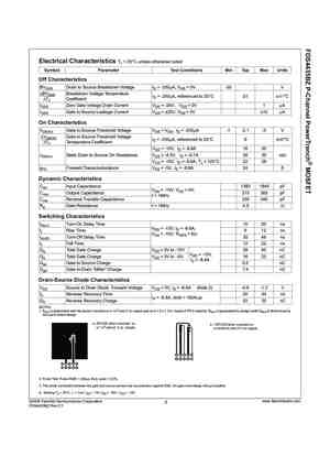
FDS4465 Datasheet (PDF)
1.1. fds4465.pdf Size:137K _fairchild_semi


March 2003
FDS4465
P-Channel 1.8V Specified PowerTrench MOSFET
General Description Features
This P-Channel 1.8V specified MOSFET is a rugged
• –13.5 A, –20 V. RDS(ON) = 8.5 mΩ @ VGS = –4.5 V
gate version of Fairchild Semiconductor’s advanced
RDS(ON) = 10.5 mΩ @ VGS = –2.5 V
PowerTrench process. It has been optimized for power
RDS(ON) = 14 m
1.2. fds4465 f085.pdf Size:400K _fairchild_semi


February 2010
tm
FDS4465_F085
P-Channel 1.8V Specified PowerTrench MOSFET
General Description Features
This P-Channel 1.8V specified MOSFET is a rugged
• –13.5 A, –20 V. RDS(ON) = 8.5 mΩ @ VGS = –4.5 V
gate version of Fairchild Semiconductor’s advanced
RDS(ON) = 10.5 mΩ @ VGS = –2.5 V
PowerTrench process. It has been optimized for power
RDS(
5.1. fds4410a.pdf Size:112K _upd-mosfet
May 2005
FDS4410A
Single N-Channel, Logic-Level, PowerTrench MOSFET
Features General Description
■ 10 A, 30 V. RDS(ON) = 13.5 mΩ @ VGS = 10 V This N-Channel Logic Level MOSFET is produced using Fair-
RDS(ON) = 20 mΩ @ VGS = 4.5 V child Semiconductor’s advanced PowerTrench process that has
been especially tailored to minimize the on-state resistance and
■ Fast switching speed
5.2. fds4480.pdf Size:144K _fairchild_semi


May 2013
FDS4480
40V N-Channel PowerTrench MOSFET
General Description Features
This N-Channel MOSFET has been designed
• 10.8 A, 40 V. RDS(ON) = 12 mΩ @ VGS = 10 V
specifically to improve the overall efficiency of DC/DC
converters using either synchronous or conventional
• Low gate charge (29 nC)
switching PWM controllers. It has been optimized for
low gate char
5.3. fds4410a.pdf Size:112K _fairchild_semi


May 2005
FDS4410A
Single N-Channel, Logic-Level, PowerTrench MOSFET
Features General Description
■ 10 A, 30 V. RDS(ON) = 13.5 mΩ @ VGS = 10 V This N-Channel Logic Level MOSFET is produced using Fair-
RDS(ON) = 20 mΩ @ VGS = 4.5 V child Semiconductor’s advanced PowerTrench process that has
been especially tailored to minimize the on-state resistance and
■ Fast switching speed
5.4. fds4470.pdf Size:146K _fairchild_semi


December 2006
FDS4470
40V N-Channel PowerTrench MOSFET
General Description Features
This N-Channel MOSFET has been designed
• 12.5 A, 40 V. RDS(ON) = 9 mΩ @ VGS = 10 V
specifically to improve the overall efficiency of DC/DC
converters using either synchronous or conventional
• Low gate charge (45 nC)
switching PWM controllers. It has been optimized for
low gate charge
5.5. fds4435bz.pdf Size:225K _fairchild_semi

April 2009
FDS4435BZ
P-Channel PowerTrench MOSFET
-30V, -8.8A, 20m
Features General Description
Max rDS(on) = 20m at VGS = -10V, ID = -8.8A This P-Channel MOSFET is produced using Fairchild
Max rDS(on) = 35m at VGS = -4.5V, ID = -6.7A Semiconductor’s advanced PowerTrench process that has
Extended VGSS range (-25V) for battery applications been especially tailored to minimi
5.6. fds4488.pdf Size:69K _fairchild_semi


December 2001
FDS4488
30V N-Channel PowerTrench MOSFET
General Description Features
This N MOSFET is produced using Fairchild
-Channel
• 7.9 A, 30 V. R = 22 mΩ @ V = 10 V
DS(ON) GS
Semiconductor’s advanced PowerTrench process that
R = 30 mΩ @ V = 4.5 V
DS(ON) GS
has been especially tailored to minimize on-state
resistance and yet maintain superior switching
•
5.7. fds4435.pdf Size:64K _fairchild_semi

October 2001
FDS4435
30V P-Channel PowerTrench MOSFET
General Description Features
This P MOSFET is a rugged gate version of
-Channel
• –8.8 A, –30 V R = 20 mΩ @ V = –10 V
DS(ON) GS
Fairchild Semiconductor’s advanced PowerTrench
R = 35 mΩ @ V = –4.5 V
DS(ON) GS
process. It has been optimized for power management
applications requiring a wide range of gave
5.8. fds4435a.pdf Size:172K _fairchild_semi

October 2001
FDS4435A
P-Channel Logic Level PowerTrench MOSFET
General Description
Features
This P-Channel Logic Level MOSFET is produced using • -9 A, -30 V. RDS(ON) = 0.017 W @ VGS = -10 V
Fairchild Semiconductor’s advanced PowerTrench process
RDS(ON) = 0.025 W @ VGS = -4.5 V
that has been especially tailored to minimize the on-state
resistance and yet maintain low gate charg
5.9. fds4435bz f085.pdf Size:296K _fairchild_semi


July 2009
FDS4435BZ_F085
P-Channel PowerTrench MOSFET
-30V, -8.8A, 20m
Features General Description
Max rDS(on) = 20m at VGS = -10V, ID = -8.8A This P-Channel MOSFET is produced using Fairchild
Max rDS(on) = 35m at VGS = -4.5V, ID = -6.7A Semiconductor’s advanced PowerTrench process that has
Extended VGSS range (-25V) for battery applications been especially tailored to mi
AO4916 Datasheet (PDF)
1.1. ao4916.pdf Size:651K _update
AO4916
30V Dual N-Channel MOSFET with Schottky Diode
General Description Product Summary
The AO4916 uses advanced trench technology to provide
Q1(N-Channel) Q2(N-Channel)
excellent RDS(ON) and low gate charge. The two MOSFETs
VDS= 30V 30V
make a compact and efficient switch and synchronous
ID= 8A (VGS=10V) 8A (VGS=10V)
rectifier combination for use in DC-DC converters. A
RDS(ON) 1.2. ao4916l.pdf Size:370K _update
Rev 3: Nov 2004
AO4916, AO4916L( Green Product )
Dual N-Channel Enhancement Mode Field Effect Transistor
with Schottky Diode
General Description Features
VDS (V) = 30V
The AO4916 uses advanced trench technology to
ID = 8.5A
provide excellent R DS(ON) and low gate charge. The
RDS(ON)
1.3. ao4916.pdf Size:651K _aosemi
AO4916
30V Dual N-Channel MOSFET with Schottky Diode
General Description Product Summary
The AO4916 uses advanced trench technology to provide
Q1(N-Channel) Q2(N-Channel)
excellent RDS(ON) and low gate charge. The two MOSFETs
VDS= 30V 30V
make a compact and efficient switch and synchronous
ID= 8A (VGS=10V) 8A (VGS=10V)
rectifier combination for use in DC-DC converters. A
RDS(ON) 1.4. ao4916l.pdf Size:370K _aosemi
Rev 3: Nov 2004
AO4916, AO4916L( Green Product )
Dual N-Channel Enhancement Mode Field Effect Transistor
with Schottky Diode
General Description Features
VDS (V) = 30V
The AO4916 uses advanced trench technology to
ID = 8.5A
provide excellent R DS(ON) and low gate charge. The
RDS(ON)
AO4468 MOSFET — описание производителя. Даташиты. Основные параметры и характеристики. Поиск аналога. Справочник
Наименование прибора: AO4468
Тип транзистора: MOSFET
Полярность: N
Максимальная рассеиваемая мощность (Pd): 3.1
W
Предельно допустимое напряжение сток-исток (Uds): 30
V
Предельно допустимое напряжение затвор-исток (Ugs): 20
V
Пороговое напряжение включения Ugs(th): 2.4
V
Максимально допустимый постоянный ток стока (Id): 10.5
A
Максимальная температура канала (Tj): 150
°C
Время нарастания (tr): 3.5
ns
Выходная емкость (Cd): 110
pf
Сопротивление сток-исток открытого транзистора (Rds): 0.017
Ohm
Тип корпуса: SO-8
AO4468
Datasheet (PDF)
1.1. ao4468.pdf Size:315K _aosemi
AO4468
30V N-Channel MOSFET
General Description Product Summary
VDS
30V
The AO4468 combines advanced trench MOSFET
technology with a low resistance package to provide
ID (at VGS=10V) 10.5A
extremely low RDS(ON). This device is ideal for load switch
RDS(ON) (at VGS=10V) 1.2. ao4468.pdf Size:1303K _kexin
SMD Type MOSFET
N-Channel MOSFET
AO4468 (KO4468)
SOP-8
■ Features
● VDS (V) = 30V
1.50 0.15
● ID = 10.5 A (VGS = 10V)
● RDS(ON) < 17mΩ (VGS = 10V)
1 Source 5 Drain
● RDS(ON) < 23mΩ (VGS = 4.5V)
6 Drain
2 Source
7 Drain
3 Source
8 Drain
4 Gate
D
G
S
■ Absolute Maximum Ratings Ta = 25℃
Parameter Symbol Rating Unit
Drain-Source Voltage VDS 30
V
Gat
5.1. ao4466l.pdf Size:199K _update-mosfet
AO4466
N-Channel Enhancement Mode Field Effect Transistor
General Description Features
The AO4466/L uses advanced trench technology to VDS (V) = 30V
provide excellent RDS(ON) and low gate charge. This
ID = 9.4A (VGS = 10V)
device is suitable for use as a load switch or in PWM
RDS(ON) 5.2. ao4466.pdf Size:324K _aosemi
AO4466
30V N-Channel MOSFET
General Description Product Summary
The AO4466 uses advanced trench technology to VDS (V) = 30V
provide excellent RDS(ON) and low gate charge. This ID = 10A (VGS = 10V)
device is suitable for use as a load switch or in PWM
RDS(ON)
5.3. ao4466l.pdf Size:199K _aosemi
AO4466
N-Channel Enhancement Mode Field Effect Transistor
General Description Features
The AO4466/L uses advanced trench technology to VDS (V) = 30V
provide excellent RDS(ON) and low gate charge. This
ID = 9.4A (VGS = 10V)
device is suitable for use as a load switch or in PWM
RDS(ON) 5.4. ao4466.pdf Size:1389K _kexin
SMD Type MOSFET
N-Channel MOSFET
AO4466 (KO4466)
SOP-8
■ Features
● VDS (V) = 30V
● ID = 9.4 A (VGS = 10V)
1.50 0.15
● RDS(ON) < 23mΩ (VGS = 10V)
● RDS(ON) < 35mΩ (VGS = 4.5V)
1 Source 5 Drain
6 Drain
2 Source
7 Drain
3 Source
8 Drain
4 Gate
D
G
S
■ Absolute Maximum Ratings Ta = 25℃
Parameter Symbol Rating Unit
Drain-Source Voltage VDS 30
V
Gate
Другие MOSFET… SID40N03
, SID9435
, SID9575
, SID9971
, SJV01N60
, SMG1330N
, SMG2301
, SMG2301P
, IRF540N
, SMG2302N
, SMG2305
, SMG2305P
, SMG2305PE
, SMG2306A
, SMG2306N
, SMG2306NE
, SMG2310A
.
FDS4685 MOSFET — описание производителя. Даташиты. Основные параметры и характеристики. Поиск аналога. Справочник
Наименование прибора: FDS4685
Тип транзистора: MOSFET
Полярность: P
Максимальная рассеиваемая мощность (Pd): 2.5
W
Предельно допустимое напряжение сток-исток (Uds): 40
V
Предельно допустимое напряжение затвор-исток (Ugs): 20
V
Пороговое напряжение включения Ugs(th): 3
V
Максимально допустимый постоянный ток стока (Id): 8.2
A
Максимальная температура канала (Tj): 150
°C
Общий заряд затвора (Qg): 19
nC
Сопротивление сток-исток открытого транзистора (Rds): 0.027
Ohm
Тип корпуса: SOIC
FDS4685
Datasheet (PDF)
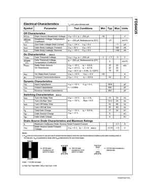
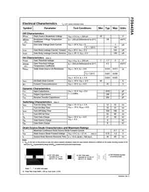
1.1. fds4685.pdf Size:506K _fairchild_semi


June 2005
FDS4685
40V P-Channel PowerTrench MOSFET
Features Applications
■ –8.2 A, –40 V RDS(ON) = 0.027 Ω @ VGS = –10 V ■ Power management
RDS(ON) = 0.035 Ω @ VGS = –4.5 V
■ Load switch
■ Fast switching speed
■ Battery protection
■ High performance trench technology for extremely low
RDS(ON)
General Description
■ High power and current handling capabi
5.1. fds4675.pdf Size:73K _fairchild_semi


February 2001
FDS4675
40V P-Channel PowerTrench MOSFET
General Description Features
This P MOSFET is a rugged gate version of
-Channel
• –11 A, –40 V R = 0.013 Ω @ V = –10 V
DS(ON) GS
Fairchild Semiconductor’s advanced PowerTrench
R = 0.017 Ω @ V = –4.5 V
DS(ON) GS
process. It has been optimized for power management
applications requiring a wide range of g
5.2. fds4675 f085.pdf Size:310K _fairchild_semi


February 2010
tm
FDS4675_F085
40V P-Channel PowerTrench MOSFET
General Description Features
This P MOSFET is a rugged gate version of
-Channel
• –11 A, –40 V R = 0.013 Ω @ V = –10 V
DS(ON) GS
Fairchild Semiconductor’s advanced PowerTrench
R = 0.017 Ω @ V = –4.5 V
DS(ON) GS
process. It has been optimized for power management
applications requiring a wide ra
5.3. fds4672a.pdf Size:439K _fairchild_semi


February 2007
tm
FDS4672A
40V N-Channel PowerTrench MOSFET
General Description Features
This N-Channel MOSFET has been designed
• 11 A, 40 V. RDS(ON) = 13 mΩ @ VGS = 4.5 V
specifically to improve the overall efficiency of DC/DC
converters using either synchronous or conventional
• High performance trench technology for extremely
switching PWM controllers. It has been op
Другие MOSFET… STB458D
, STB440S
, FDS4559
, STB438S
, FDS4559_F085
, STB438A
, FDS4672A
, FDS4675_F085
, TPC8107
, FDS4897AC
, STB434S
, FDS4897C
, STB432S
, FDS4935A
, FDS4935BZ
, FDS5351
, FDS5670
.
Биполярный транзистор 2SC4407 — описание производителя. Основные параметры. Даташиты.
Наименование производителя: 2SC4407
Тип материала: Si
Полярность: NPN
Максимальная рассеиваемая мощность (Pc): 0.1
W
Макcимально допустимое напряжение коллектор-база (Ucb): 25
V
Макcимальный постоянный ток коллектора (Ic): 0.05
A
Предельная температура PN-перехода (Tj): 125
°C
Граничная частота коэффициента передачи тока (ft): 3000
MHz
Статический коэффициент передачи тока (hfe): 40
Корпус транзистора: TO236
2SC4407
Datasheet (PDF)
1.1. 2sc4407.pdf Size:105K _sanyo
Ordering number:EN2760
NPN Epitaxial Planar Silicon Transistor
2SC4407
VHF/UHF Mixer,
Local Oscillator Applications
Applications Package Dimensions
VHF/UHF mixers, frequency converters, local
unit:mm
oscillators.
2059B
0.3
Features
0.15
High cutoff frequency : fT=3.0GHz typ
3
High power gain : PG=12dB typ (f=0.9GHz)
0~0.1
Small noise figure : NF=3.0dB typ (f
4.1. 2sc4409.pdf Size:150K _toshiba
2SC4409
TOSHIBA Transistor Silicon NPN Epitaxial Type (PCT Process)
2SC4409
Power Amplifier Applications
Unit: mm
Power switching applications
• Low collector saturation voltage: VCE (sat) = 0.5V (max) (at I = 1A)
C
• High speed switching time: t = 500ns (typ.)
stg
• Small flat package
• P = 1~2 W (Mounted on ceramic substrate)
C
• Complementary to 2SA1681
Ma
4.2. 2sc4408.pdf Size:186K _toshiba
4.3. 2sc4404.pdf Size:113K _sanyo
Ordering number:EN2757
NPN Epitaxial Planar Silicon Transistor
2SC4404
UHF Local Oscillator,
Wide-Band Amplifier Applications
Applications Package Dimensions
UHF OSC, wide-band amplifiers. unit:mm
2059B
Features
0.3
High cutoff frequency : fT=5.0GHz typ
0.15
High power gain : MAG=14dB typ (f=0.9GHz)
3
Small noise figure : NF=2.2dB typ (f=0.9GHz)
0~0.1
Very
4.4. 2sc4406.pdf Size:105K _sanyo
Ordering number:EN2759A
NPN Epitaxial Planar Silicon Transistor
2SC4406
VHF Frequency Mixer,
Local Oscillator Applications
Applications Package Dimensions
VHF mixer, frequency converters, local oscillators. unit:mm
2059B
Features
0.3
High cutoff frequency : fT=1.2GHz typ
0.15
High power gain : PG=15dB typ (f=0.4GHz)
3
Good dependence of fT on current.
0~0.1
4.5. 2sc4405.pdf Size:112K _sanyo
Ordering number:EN2758
NPN Epitaxial Planar Silicon Transistor
2SC4405
UHF, Low-Noise,
Wide-Band Amplifier Applications
Applications Package Dimensions
UHF, low-noise amplifiers, wide-band amplifiers. unit:mm
2059B
Features
0.3
High cutoff frequency : fT=5.0GHz typ
0.15
High power gain : MAG=14dB typ (f=0.9GHz)
3
Small noise figure : NF=1.5dB typ (f=0.9GHz)
0~0
4.6. 2sc4403.pdf Size:112K _sanyo
Ordering number:EN2756
NPN Epitaxial Planar Silicon Transistor
2SC4403
VHF/UHF Local Oscillator Applications
Applications Package Dimensions
VHF/UHF oscillators. unit:mm
2059B
Features
0.3
High cutoff frequency : fT=3.0GHz typ
0.15
High power gain : MAG=12dB typ (f=0.9GHz)
3
Small noise figure : NF=2.5dB typ (f=0.9GHz)
0~0.1
Very small-sized package permitti
4.7. 2sc4400.pdf Size:79K _sanyo
Ordering number:EN3195
NPN Epitaxial Planar Silicon Transistor
2SC4400
High-Frequency
General-Purpose Amplifier Applications
Features Package Dimensions
High power gain.
unit:mm
High cutoff frequency.
2059B
Small Cob, Cre.
Very small-sized package permitting the 2SC4400-
0.3
0.15
applied sets to be made small and slim.
3
0~0.1
1 2
0.3 0.6
0.65 0.65
0.9
2
4.8. 2sc4401.pdf Size:119K _sanyo
Ordering number:EN2754
NPN Epitaxial Planar Silicon Transistor
2SC4401
VHF/UHF Mixer, Local Oscillator,
Low-Voltage Amplifier Applications
Applications Package Dimensions
VHF/UHF MIX/OSC, low-voltage high-frequency
unit:mm
amplifiers.
2059B
0.3
Features
0.15
Low-voltage operation
3
: fT=3.0GHz typ (VCE=3V)
0~0.1
: MAG=11dB typ (VCE=3V, IC=3mA)
: NF=3.0dB typ (VCE
4.9. 2sc4402.pdf Size:120K _sanyo
Ordering number:EN2755
NPN Epitaxial Planar Silicon Transistor
2SC4402
VHF/UHF Mixer, Local Oscillator,
Low-Voltage Amplifier Applications
Applications Package Dimensions
VHF/UHF MIX/OSC, low-voltage high-frequency
unit:mm
amplifiers.
2059B
0.3
Features
0.15
Low-voltage operation
3
: fT=3.0GHz typ (VCE=3V)
0~0.1
: MAG=12dB typ (VCE=3V, IC=10mA)
: NF=1.5dB typ (VC
4.10. 2sc4409.pdf Size:1046K _kexin
SMD Type Transistors
NPN Transistors
2SC4409
1.70 0.1
■ Features
● Low collector saturation voltage
● High speed switching time
● Small flat package
0.42 0.1
0.46 0.1
● PC = 1~2 W (Mounted on a ceramic substrate)
● Complementary to 2SA1681
1.Base
2.Collector
3.Emitter
■ Absolute Maximum Ratings Ta = 25℃
Parameter Symbol Rating Unit
Collector — Base Voltage
Другие транзисторы… 2SC4360
, 2SC4361
, 2SC4362
, 2SC4363
, 2SC4364
, 2SC4365
, 2SC4366
, 2SC4367
, D882
, 2SC4369
, 2SC437
, 2SC4370
, 2SC4371
, 2SC4372
, 2SC4373
, 2SC4374
, 2SC4375
.
AO4478 MOSFET — описание производителя. Даташиты. Основные параметры и характеристики. Поиск аналога. Справочник
Наименование прибора: AO4478
Тип транзистора: MOSFET
Полярность: N
Максимальная рассеиваемая мощность (Pd): 3.1
W
Предельно допустимое напряжение сток-исток (Uds): 30
V
Предельно допустимое напряжение затвор-исток (Ugs): 25
V
Пороговое напряжение включения Ugs(th): 2
V
Максимально допустимый постоянный ток стока (Id): 9
A
Максимальная температура канала (Tj): 150
°C
Время нарастания (tr): 8
ns
Выходная емкость (Cd): 90
pf
Сопротивление сток-исток открытого транзистора (Rds): 0.019
Ohm
Тип корпуса: SO-8
AO4478
Datasheet (PDF)
1.1. ao4478.pdf Size:192K _aosemi


AO4478
30V N-Channel MOSFET
General Description Product Summary
The AO4478 uses advanced trench technology to VDS (V) = 30V
provide excellent RDS(ON), low gate charge. This
ID = 9A (VGS = 10V)
device is suitable for use as general puspose, PWM and
RDS(ON) 1.2. ao4478.pdf Size:1096K _kexin


SMD Type MOSFET
N-Channel MOSFET
AO4478 (KO4478)
SOP-8
■ Features
● VDS (V) = 30V
● ID = 9 A (VGS = 10V)
1.50 0.15
● RDS(ON) < 19mΩ (VGS = 10V)
● RDS(ON) < 26mΩ (VGS = 4.5V)
1 Source 5 Drain
6 Drain
2 Source
7 Drain
3 Source
8 Drain
4 Gate
D
G
S
■ Absolute Maximum Ratings Ta = 25℃
Parameter Symbol Rating Unit
Drain-Source Voltage VDS 30
V
Gate-S
5.1. ao4472.pdf Size:158K _update
AO4472
N-Channel Enhancement Mode Field Effect Transistor
General Description
Features
The AO4472 uses advanced trench technology to provide
VDS (V) = 30V
excellent RDS(ON), shoot-through immunity, body diode
www.DataSheet4U.com
ID = 19A (VGS = 10V)
characteristics and ultra-low gate resistance. This device is
RDS(ON) 5.2. ao4474.pdf Size:129K _update
AO4474
N-Channel Enhancement Mode Field Effect Transistor
General Description Features
The AO4474/L uses advanced trench technology to
provide excellent RDS(ON), low gate charge.This device VDS (V) = 30V
is suitable for use as a high side switch in SMPS and ID = 13.4A (VGS = 10V)
general purpose applications.
RDS(ON)
5.3. ao4476a.pdf Size:365K _aosemi


AO4476A
30V N-Channel MOSFET
General Description Product Summary
VDS
30V
The AO4476A combines advanced trench MOSFET
technology with a low resistance package to provide
ID (at VGS=10V) 15A
extremely low RDS(ON). This device is suitable for use as a
RDS(ON) (at VGS=10V) 5.4. ao4472.pdf Size:158K _aosemi


AO4472
N-Channel Enhancement Mode Field Effect Transistor
General Description
Features
The AO4472 uses advanced trench technology to provide
VDS (V) = 30V
excellent RDS(ON), shoot-through immunity, body diode
www.DataSheet4U.com
ID = 19A (VGS = 10V)
characteristics and ultra-low gate resistance. This device is
RDS(ON)
5.5. ao4474.pdf Size:129K _aosemi


AO4474
N-Channel Enhancement Mode Field Effect Transistor
General Description Features
The AO4474/L uses advanced trench technology to
provide excellent RDS(ON), low gate charge.This device VDS (V) = 30V
is suitable for use as a high side switch in SMPS and ID = 13.4A (VGS = 10V)
general purpose applications.
RDS(ON) 5.6. ao4476a.pdf Size:2008K _kexin


SMD Type MOSFET
N-Channel MOSFET
AO4476A (KO4476A)
SOP-8
■ Features
● VDS (V) = 30V
● ID = 15 A (VGS = 10V)
● RDS(ON) < 7.7mΩ (VGS = 10V)
1.50 0.15
● RDS(ON) < 10.8mΩ (VGS = 4.5V)
1 Source 5 Drain
6 Drain
2 Source
7 Drain
3 Source
8 Drain
4 Gate
D
G
S
■ Absolute Maximum Ratings Ta = 25℃
Parameter Symbol Rating Unit
Drain-Source Voltage VDS 30
V
5.7. ao4476.pdf Size:1222K _kexin


SMD Type MOSFET
N-Channel MOSFET
AO4476 (KO4476)
SOP-8
■ Features
● VDS (V) = 30V
● ID = 15 A (VGS = 10V)
● RDS(ON) < 10.5mΩ (VGS = 10V)
1.50 0.15
● RDS(ON) < 17mΩ (VGS = 4.5V)
1 Source 5 Drain
6 Drain
2 Source
7 Drain
3 Source
8 Drain
4 Gate
D
G
S
■ Absolute Maximum Ratings Ta = 25℃
Parameter Symbol Rating Unit
Drain-Source Voltage VDS 30
V
Ga
Другие MOSFET… SID40N03
, SID9435
, SID9575
, SID9971
, SJV01N60
, SMG1330N
, SMG2301
, SMG2301P
, IRF540N
, SMG2302N
, SMG2305
, SMG2305P
, SMG2305PE
, SMG2306A
, SMG2306N
, SMG2306NE
, SMG2310A
.