Datasheet spa20n60c3 — infineon даташит полевой транзистор, n, coolmos, to-220
Содержание:
- SPP20N65C3 Datasheet (PDF)
- SPW47N60C3 Datasheet (PDF)
- SPP20N60C3 Datasheet (PDF)
- SPA20N60C3 Datasheet (PDF)
- FCP20N60 Datasheet (PDF)
- SPU02N60C3 Datasheet (PDF)
- SPP20N60S5 Datasheet (PDF)
- CS20N60_A8H Datasheet (PDF)
- SPW20N60C3 Datasheet (PDF)
- SPW20N60S5 Datasheet (PDF)
- FCA20N60S Datasheet (PDF)
- CS1N60_C3H Datasheet (PDF)
- CS20N60_A8H MOSFET — описание производителя. Даташиты. Основные параметры и характеристики. Поиск аналога. Справочник
- CS20N60_A8H Datasheet (PDF)
- SPI20N60CFD Datasheet (PDF)
SPP20N65C3 Datasheet (PDF)
1.1. spp20n65c3 spa20n65c3 spi20n65c3.pdf Size:1938K _infineon
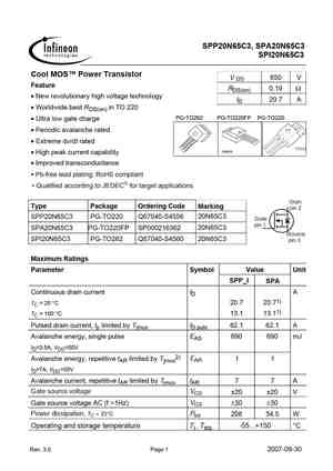
SPP20N65C3, SPA20N65C3
SPI20N65C3
Cool MOS Power Transistor
V 650 V
DS
Feature
RDS(on) 0.19 Ω
• New revolutionary high voltage technology
ID 20.7 A
• Worldwide best RDS(on) in TO 220
PG-TO262 PG-TO220FP PG-TO220
• Ultra low gate charge
• Periodic avalanche rated
3
• Extreme dv/dt rated
2
1
P-TO220-3-31
• High peak current capability
• Improved transconducta
1.2. spp20n65c3.pdf Size:247K _inchange_semiconductor
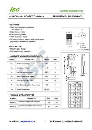

isc N-Channel MOSFET Transistor SPP20N65C3,ISPP20N65C3
·FEATURES
·Static drain-source on-resistance:
RDS(on) ≤0.19Ω
·Enhancement mode
·Fast Switching Speed
·100% avalanche tested
·Minimum Lot-to-Lot variations for robust device
performance and reliable operation
·DESCRIPTION
·Ultra low gate charge
·High peak current capability
·ABSOLUTE MAXIMUM RATINGS(T =25℃)
a
3.1. spp20n60c3 spi20n60c3 spa20n60c3 rev3.2.pdf Size:683K _infineon
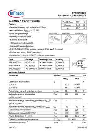
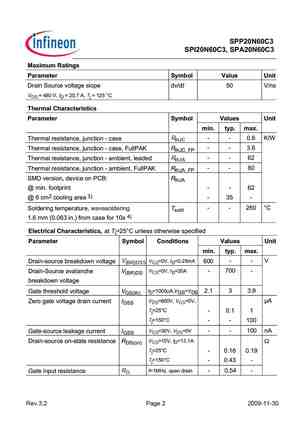
SPP20N60C3
SPI20N60C3, SPA20N60C3
Cool MOS Power Transistor
VDS @ Tjmax 650 V
Feature
RDS(on) 0.19 Ω
• New revolutionary high voltage technology
ID 20.7 A
• Worldwide best RDS(on) in TO 220
PG-TO220FP PG-TO262 PG-TO220
• Ultra low gate charge
• Periodic avalanche rated
3
• Extreme dv/dt rated
2
1
P-TO220-3-31
• High peak current capability
• Improved transco
3.2. spp20n60s5.pdf Size:129K _infineon
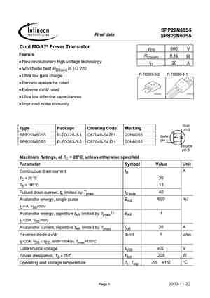
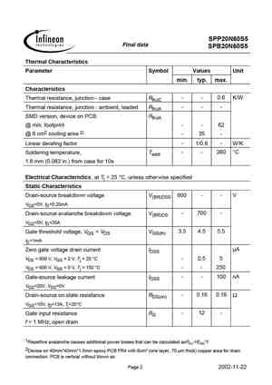
SPP20N60S5
Final data
SPB20N60S5
Cool MOS Power Transistor
VDS 600 V
Feature
RDS(on) 0.19 Ω
• New revolutionary high voltage technology
ID 20 A
• Worldwide best RDS(on) in TO 220
P-TO263-3-2 P-TO220-3-1
• Ultra low gate charge
• Periodic avalanche rated
• Extreme dv/dt rated
• Ultra low effective capacitances
• Improved noise immunity
Type Package Ordering Cod
3.3. spp20n60s5 .pdf Size:370K _infineon
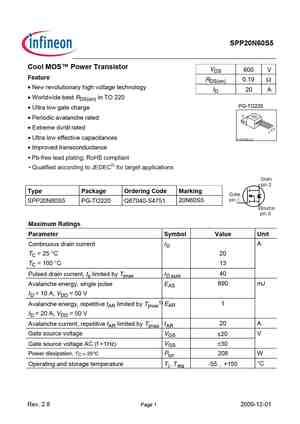
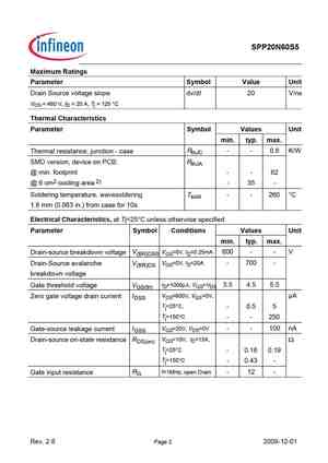
SPP20N60S5
Cool MOS Power Transistor
VDS
600 V
Feature
RDS(on) 0.19 Ω
• New revolutionary high voltage technology
ID 20 A
• Worldwide best RDS(on) in TO 220
PG-TO220
• Ultra low gate charge
2
• Periodic avalanche rated
• Extreme dv/dt rated
3
2
1
• Ultra low effective capacitances
P-TO220-3-1
• Improved transconductance
Type Package Ordering Code Marking
3.4. spp20n60c3 spi20n60c3 spa20n60c3.pdf Size:1832K _infineon
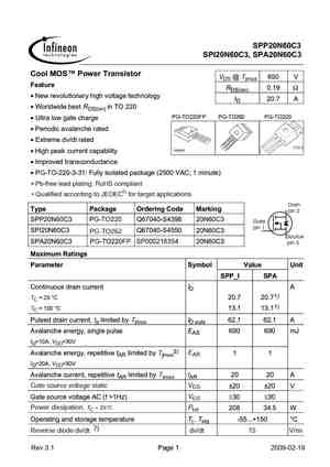
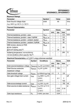
SPP20N60C3
SPI20N60C3, SPA20N60C3
Cool MOS Power Transistor
VDS @ Tjmax 650 V
Feature
RDS(on) 0.19 Ω
• New revolutionary high voltage technology
ID 20.7 A
• Worldwide best RDS(on) in TO 220
PG-TO220FP PG-TO262 PG-TO220
• Ultra low gate charge
• Periodic avalanche rated
3
• Extreme dv/dt rated
2
1
P-TO220-3-31
• High peak current capability
• Improved transco
3.5. spp20n60cfd.pdf Size:643K _infineon
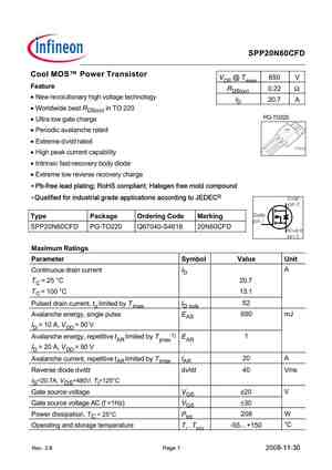
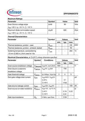
SPP20N60CFD
CססI MOS Pסwer Transistסr
VDS @ Tjmax 650 V
Feature
RDS(on) 0.22
• New revolutionary high voltage technology
ID 20.7 A
• Worldwide best RDS(on) in TO 220
PG-TO220
• Ultra low gate charge
• Periodic avalanche rated
• Extreme dv/dt rated
• High peak current capability
• Intrinsic fast-recovery body diode
• Extreme low reverse recovery charge
Type Pa
3.6. spp20n60s5.pdf Size:246K _inchange_semiconductor
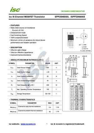

isc N-Channel MOSFET Transistor SPP20N60S5,ISPP20N60S5
·FEATURES
·Static drain-source on-resistance:
RDS(on) ≤0.19Ω
·Enhancement mode
·Fast Switching Speed
·100% avalanche tested
·Minimum Lot-to-Lot variations for robust device
performance and reliable operation
·DESCRIPTION
·Ultra low gate charge
·Ultra low effective capacitance
·Improved transconductance
·ABSOLUT
3.7. spp20n60c3.pdf Size:247K _inchange_semiconductor
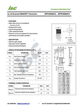

isc N-Channel MOSFET Transistor SPP20N60C3,ISPP20N60C3
·FEATURES
·Static drain-source on-resistance:
RDS(on) ≤0.19Ω
·Enhancement mode
·Fast Switching Speed
·100% avalanche tested
·Minimum Lot-to-Lot variations for robust device
performance and reliable operation
·DESCRIPTION
·Ultra low gate charge
·High peak current capability
·Improved transconductance
·ABSOLUTE M
3.8. spp20n60cfd.pdf Size:247K _inchange_semiconductor
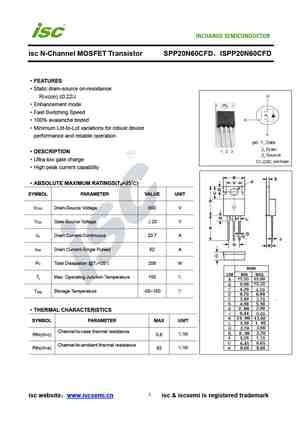

isc N-Channel MOSFET Transistor SPP20N60CFD,ISPP20N60CFD
·FEATURES
·Static drain-source on-resistance:
RDS(on) ≤0.22Ω
·Enhancement mode
·Fast Switching Speed
·100% avalanche tested
·Minimum Lot-to-Lot variations for robust device
performance and reliable operation
·DESCRIPTION
·Ultra low gate charge
·High peak current capability
·ABSOLUTE MAXIMUM RATINGS(T =25℃)
a
SPW47N60C3 Datasheet (PDF)
1.1. spw47n60cfd.pdf Size:616K _infineon
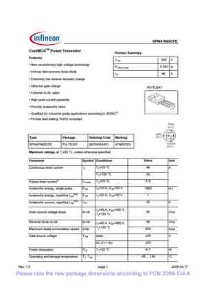
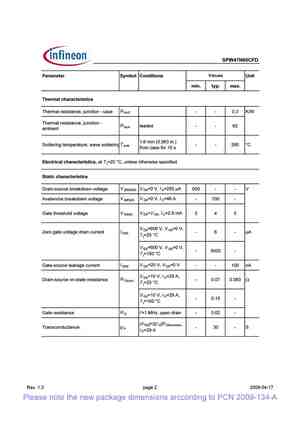
SPW47N60CFD
TM
CססIMOSTM «9@/; %;+8-= $>77+;B
Features
V
—
R (7H C7GA>FE;A@3CJ :;9: GA>E397 E75:@A>A9J
DS(on) max
R $@EC;@D;5 83DE C75AG7CJ 4A6J 6;A67
46 A
46
D
R IEC7?7>J >AH C7G7CD7 C75AG7CJ 5:3C97
R / >EC3 >AH 93E7 5:3C97
PG‐TO247
R IEC7?7 6v /dt C3E76
/d
R #;9: B73= 5FCC7@E 53B34;>;EJ
R *7C;A6;5 3G3>3@5:7 C3E76
R + F3>;8;76 355AC6;@9 EA %
R *4 8C77
1.2. spw47n60c3.pdf Size:828K _infineon
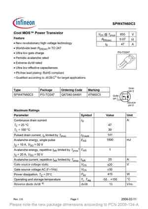
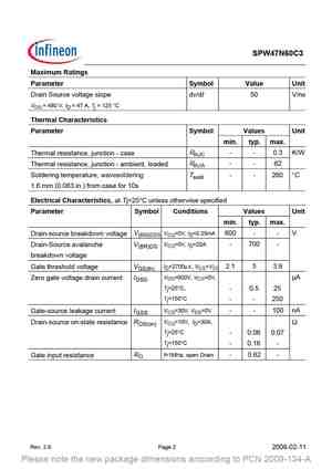
VDS Tjmax
Ω
•
•
G
•
•
•
•
G
1.3. spw47n60cfd.pdf Size:243K _inchange_semiconductor
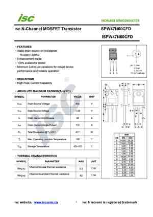
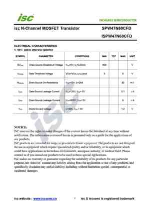
INCHANGE Semiconductor
isc N-Channel MOSFET Transistor SPW47N60CFD
ISPW47N60CFD
·FEATURES
·Static drain-source on-resistance:
RDS(on)≤83mΩ
·Enhancement mode:
·100% avalanche tested
·Minimum Lot-to-Lot variations for robust device
performance and reliable operation
·DESCRITION
·High Peak Current Capability
·ABSOLUTE MAXIMUM RATINGS(T =25℃)
a
SYMBOL PARAMETER VALUE UNI
1.4. spw47n60c3.pdf Size:244K _inchange_semiconductor

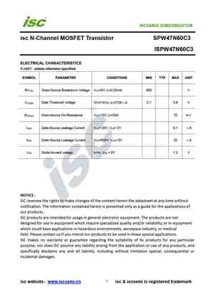
isc N-Channel MOSFET Transistor SPW47N60C3
ISPW47N60C3
·FEATURES
·Static drain-source on-resistance:
RDS(on)≤70mΩ
·Enhancement mode:
·100% avalanche tested
·Minimum Lot-to-Lot variations for robust device
performance and reliable operation
·DESCRITION
·Improved Transconductance
·ABSOLUTE MAXIMUM RATINGS(T =25℃)
a
SYMBOL PARAMETER VALUE UNIT
V Drain-Source Voltage 600
SPP20N60C3 Datasheet (PDF)
1.1. spp20n60c3 spi20n60c3 spa20n60c3 rev3.2.pdf Size:683K _infineon


SPP20N60C3
SPI20N60C3, SPA20N60C3
Cool MOS Power Transistor
VDS @ Tjmax 650 V
Feature
RDS(on) 0.19 ?
New revolutionary high voltage technology
ID 20.7 A
Worldwide best RDS(on) in TO 220
PG-TO220FP PG-TO262 PG-TO220
Ultra low gate charge
Periodic avalanche rated
3
Extreme dv/dt rated
2
1
P-TO220-3-31
High peak current capability
Improved transconductance
PG-TO-22
1.2. spp20n60cfd rev.2.6.pdf Size:643K _infineon
SPP20N60CFD
C??I MOS P?wer Transist?r
VDS @ Tjmax 650 V
Feature
RDS(on) 0.22
New revolutionary high voltage technology
ID 20.7 A
Worldwide best RDS(on) in TO 220
PG-TO220
Ultra low gate charge
Periodic avalanche rated
Extreme dv/dt rated
High peak current capability
Intrinsic fast-recovery body diode
Extreme low reverse recovery charge
Type Package Ordering C?de Mar
1.3. spp20n60c3 spi20n60c3 spa20n60c3.pdf Size:1832K _infineon


SPP20N60C3
SPI20N60C3, SPA20N60C3
Cool MOS Power Transistor
VDS @ Tjmax 650 V
Feature
RDS(on) 0.19 ?
New revolutionary high voltage technology
ID 20.7 A
Worldwide best RDS(on) in TO 220
PG-TO220FP PG-TO262 PG-TO220
Ultra low gate charge
Periodic avalanche rated
3
Extreme dv/dt rated
2
1
P-TO220-3-31
High peak current capability
Improved transconductance
PG-TO-22
1.4. spp20n60c3.pdf Size:247K _inchange_semiconductor


isc N-Channel MOSFET Transistor SPP20N60C3,ISPP20N60C3
·FEATURES
·Static drain-source on-resistance:
RDS(on) ≤0.19Ω
·Enhancement mode
·Fast Switching Speed
·100% avalanche tested
·Minimum Lot-to-Lot variations for robust device
performance and reliable operation
·DESCRIPTION
·Ultra low gate charge
·High peak current capability
·Improved transconductance
·ABSOLUTE M
1.5. spp20n60cfd.pdf Size:247K _inchange_semiconductor


isc N-Channel MOSFET Transistor SPP20N60CFD,ISPP20N60CFD
·FEATURES
·Static drain-source on-resistance:
RDS(on) ≤0.22Ω
·Enhancement mode
·Fast Switching Speed
·100% avalanche tested
·Minimum Lot-to-Lot variations for robust device
performance and reliable operation
·DESCRIPTION
·Ultra low gate charge
·High peak current capability
·ABSOLUTE MAXIMUM RATINGS(T =25℃)
a
SPA20N60C3 Datasheet (PDF)
1.1. spp20n60c3 spi20n60c3 spa20n60c3 rev3.2.pdf Size:683K _infineon


SPP20N60C3
SPI20N60C3, SPA20N60C3
Cool MOS Power Transistor
VDS @ Tjmax 650 V
Feature
RDS(on) 0.19 Ω
• New revolutionary high voltage technology
ID 20.7 A
• Worldwide best RDS(on) in TO 220
PG-TO220FP PG-TO262 PG-TO220
• Ultra low gate charge
• Periodic avalanche rated
3
• Extreme dv/dt rated
2
1
P-TO220-3-31
• High peak current capability
• Improved transco
1.2. spp20n60c3 spi20n60c3 spa20n60c3.pdf Size:1832K _infineon


SPP20N60C3
SPI20N60C3, SPA20N60C3
Cool MOS Power Transistor
VDS @ Tjmax 650 V
Feature
RDS(on) 0.19 Ω
• New revolutionary high voltage technology
ID 20.7 A
• Worldwide best RDS(on) in TO 220
PG-TO220FP PG-TO262 PG-TO220
• Ultra low gate charge
• Periodic avalanche rated
3
• Extreme dv/dt rated
2
1
P-TO220-3-31
• High peak current capability
• Improved transco
1.3. spa20n60cfd.pdf Size:466K _infineon
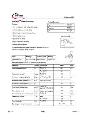
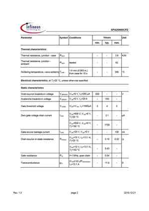
SPA20N60CFD
CoolMOSTM Power Transistor
Product Summary
Features
V 600 V
DS
• New revolutionary high voltage technology
R 0.22
DS(on),max
• Intrinsic fast-recovery body diode
1)
20.7 A
I
D
• Extremely low reverse recovery charge
• Ultra low gate charge
PG-TO220-3-31
• Extreme dv /dt rated
• High peak current capability
• Periodic avalanche rated
• Qualified f
1.4. spa20n60c3.pdf Size:201K _inchange_semiconductor
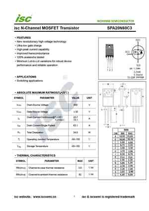
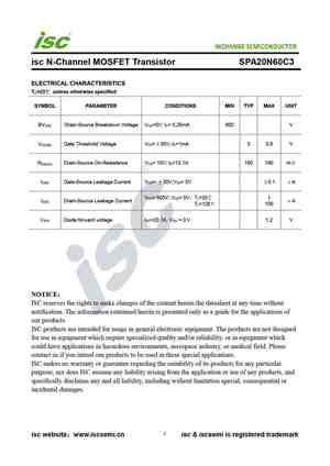
INCHANGE Semiconductor
isc N-Channel MOSFET Transistor SPA20N60C3
·FEATURES
·New revolutionary high voltage technology
·Ultra low gate charge
·High peak current capability
·Improved transconductance
·100% avalanche tested
·Minimum Lot-to-Lot variations for robust device
performance and reliable operation
·APPLICATIONS
·Switching applications
·ABSOLUTE MAXIMUM RATINGS(T =25
1.5. spa20n60cfd.pdf Size:199K _inchange_semiconductor
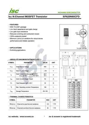
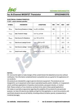
INCHANGE Semiconductor
Isc N-Channel MOSFET Transistor SPA20N60CFD
·FEATURES
·With TO-220F package
·Low input capacitance and gate charge
·Low gate input resistance
·Reduced switching and conduction losses
·100% avalanche tested
·Minimum Lot-to-Lot variations for robust device
performance and reliable operation
·APPLICATIONS
·Switching applications
·ABSOLUTE MAXIMUM RATING
FCP20N60 Datasheet (PDF)
1.1. fcp20n60fs.pdf Size:1056K _upd-mosfet
December 2008
TM
SuperFET
FCP20N60 / FCPF20N60
600V N-Channel MOSFET
Features Description
• 650V @TJ = 150°C SuperFETTM is, Fairchild’s proprietary, new generation of high
voltage MOSFET family that is utilizing an advanced charge
• Typ. RDS(on) = 0.15Ω
balance mechanism for outstanding low on-resistance and
• Ultra low gate charge (typ. Qg = 75nC) lower gate charge perfo
1.2. fcp20n60fs fcp20n60 fcpf20n60.pdf Size:1056K _fairchild_semi
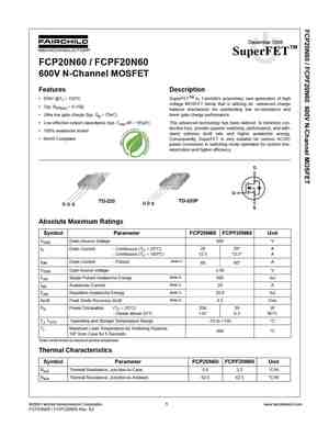
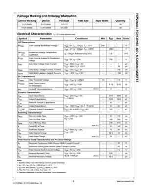
December 2008
TM
SuperFET
FCP20N60 / FCPF20N60
600V N-Channel MOSFET
Features Description
• 650V @TJ = 150°C SuperFETTM is, Fairchild’s proprietary, new generation of high
voltage MOSFET family that is utilizing an advanced charge
• Typ. RDS(on) = 0.15Ω
balance mechanism for outstanding low on-resistance and
• Ultra low gate charge (typ. Qg = 75nC) lower gate charge perfo
1.3. fcp20n60 fcpf20n60.pdf Size:613K _fairchild_semi
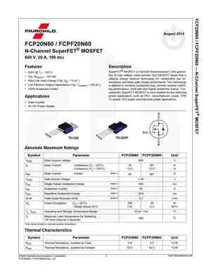
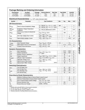
August 2014
FCP20N60 / FCPF20N60
N-Channel SuperFET MOSFET
600 V, 20 A, 190 mΩ
Features Description
SuperFET MOSFET is Fairchild Semiconductor’s first genera-
• 650V @ TJ = 150°C
tion of high voltage super-junction (SJ) MOSFET family that is
• Typ. RDS(on) = 150 mΩ
utilizing charge balance technology for outstanding low on-
• Ultra Low Gate Charge (Typ. Qg = 75 nC )
r
SPU02N60C3 Datasheet (PDF)
1.1. spd02n60c3 spu02n60c3.pdf Size:1013K _infineon
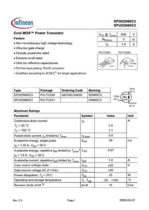
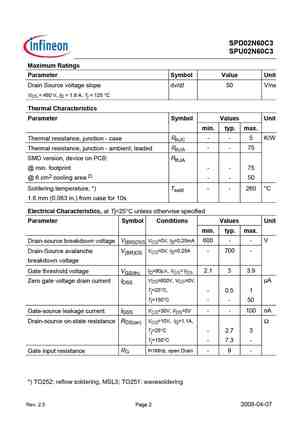
VDS Tjmax
Ω
•
•
G G
•
•
•
G
G
1.2. spu02n60c3.pdf Size:261K _inchange_semiconductor
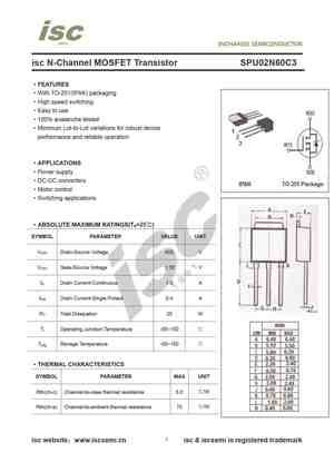
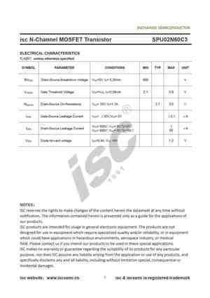
isc N-Channel MOSFET Transistor SPU02N60C3
·FEATURES
·With TO-251(IPAK) packaging
·High speed switching
·Easy to use
·100% avalanche tested
·Minimum Lot-to-Lot variations for robust device
performance and reliable operation
·APPLICATIONS
·Power supply
·DC-DC converters
·Motor control
·Switching applications
·ABSOLUTE MAXIMUM RATINGS(T =25℃)
a
SYMBOL PARAMETER VALUE
2.1. spd02n60s5 spu02n60s5.pdf Size:882K _infineon
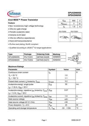
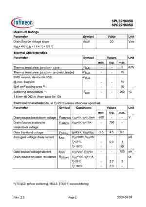
SPU02N60S5
SPD02N60S5
Cool MOS Power Transistor
VDS
600 V
Feature
RDS(on) 3 Ω
• New revolutionary high voltage technology
ID 1.8 A
• Ultra low gate charge
PG-TO252 PG-TO251
• Periodic avalanche rated
• Extreme dv/dt rated
2
3
• Ultra low effective capacitances
3
1
2
1
• Improved transconductance
Type Package Ordering Code Marking
02N60S5
SPU02N60S5 PG-TO2
2.2. spu02n60s5.pdf Size:260K _inchange_semiconductor

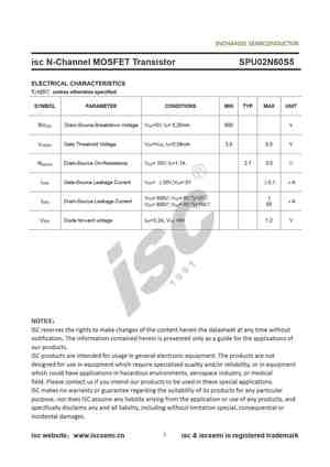
isc N-Channel MOSFET Transistor SPU02N60S5
·FEATURES
·With TO-251(IPAK) packaging
·High speed switching
·Easy to use
·100% avalanche tested
·Minimum Lot-to-Lot variations for robust device
performance and reliable operation
·APPLICATIONS
·Power supply
·DC-DC converters
·Motor control
·Switching applications
·ABSOLUTE MAXIMUM RATINGS(T =25℃)
a
SYMBOL PARAMETER VALUE
SPP20N60S5 Datasheet (PDF)
1.1. spp20n60s5.pdf Size:129K _infineon


SPP20N60S5
Final data
SPB20N60S5
Cool MOS Power Transistor
VDS 600 V
Feature
RDS(on) 0.19 Ω
• New revolutionary high voltage technology
ID 20 A
• Worldwide best RDS(on) in TO 220
P-TO263-3-2 P-TO220-3-1
• Ultra low gate charge
• Periodic avalanche rated
• Extreme dv/dt rated
• Ultra low effective capacitances
• Improved noise immunity
Type Package Ordering Cod
1.2. spp20n60s5 .pdf Size:370K _infineon


SPP20N60S5
Cool MOS Power Transistor
VDS
600 V
Feature
RDS(on) 0.19 Ω
• New revolutionary high voltage technology
ID 20 A
• Worldwide best RDS(on) in TO 220
PG-TO220
• Ultra low gate charge
2
• Periodic avalanche rated
• Extreme dv/dt rated
3
2
1
• Ultra low effective capacitances
P-TO220-3-1
• Improved transconductance
Type Package Ordering Code Marking
1.3. spp20n60s5.pdf Size:246K _inchange_semiconductor


isc N-Channel MOSFET Transistor SPP20N60S5,ISPP20N60S5
·FEATURES
·Static drain-source on-resistance:
RDS(on) ≤0.19Ω
·Enhancement mode
·Fast Switching Speed
·100% avalanche tested
·Minimum Lot-to-Lot variations for robust device
performance and reliable operation
·DESCRIPTION
·Ultra low gate charge
·Ultra low effective capacitance
·Improved transconductance
·ABSOLUT
CS20N60_A8H Datasheet (PDF)
1.1. cs20n60 anh.pdf Size:437K _crhj
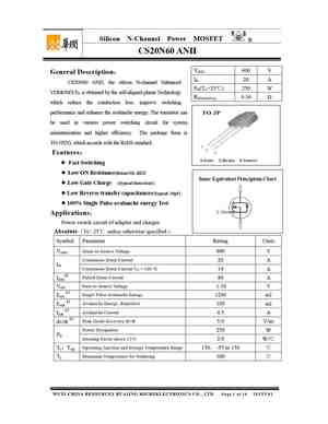

Silicon N-Channel Power MOSFET R
○
CS20N60 ANH
VDSS 600 V
General Description:
ID 20 A
CS20N60 ANH, the silicon N-channel Enhanced
PD(TC=25℃) 250 W
VDMOSFETs, is obtained by the self-aligned planar Technology
RDS(ON)Typ 0.36 Ω
which reduce the conduction loss, improve switching
performance and enhance the avalanche energy. The transistor can
be used in various po
1.2. cs20n60 a8h.pdf Size:434K _crhj
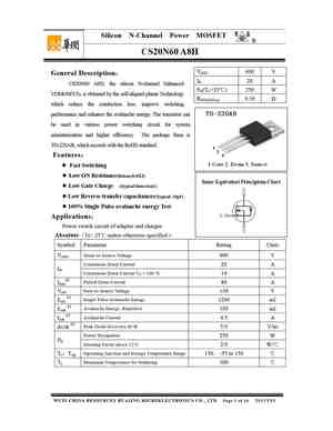

Silicon N-Channel Power MOSFET R
○
CS20N60 A8H
VDSS 600 V
General Description:
ID 20 A
CS20N60 A8H, the silicon N-channel Enhanced
PD(TC=25℃) 250 W
VDMOSFETs, is obtained by the self-aligned planar Technology
RDS(ON)Typ 0.36 Ω
which reduce the conduction loss, improve switching
performance and enhance the avalanche energy. The transistor can
be used in various po
3.1. cs20n60a8h.pdf Size:434K _update_mosfet
Silicon N-Channel Power MOSFET R
○
CS20N60 A8H
VDSS 600 V
General Description:
ID 20 A
CS20N60 A8H, the silicon N-channel Enhanced
PD(TC=25℃) 250 W
VDMOSFETs, is obtained by the self-aligned planar Technology
RDS(ON)Typ 0.36 Ω
which reduce the conduction loss, improve switching
performance and enhance the avalanche energy. The transistor can
be used in various po
3.2. cs20n60.pdf Size:109K _update_mosfet
CS20N60 型 N 沟道场效应晶体管
参数符号 测试条件 最小值 典型值 最大值 单位
PD TC=25℃ 300 W
线性降低系数 2.38 W/℃
极
ID (VGS=10V,TC=25℃) 20 A
限
VGS ±20 V
值
Tjm +150 ℃
Tstg -55 +150 ℃
热
特
RthJC 0.42 ℃/W
性
BVDSS VGS=0V,ID=0.25mA 600 V
RDS on) VGS=10V,ID=10A 0.32 0.46 Ω
(
电
VGS th) VDS=VGS,ID=0.25m
3.3. cs20n60anh.pdf Size:437K _update_mosfet
Silicon N-Channel Power MOSFET R
○
CS20N60 ANH
VDSS 600 V
General Description:
ID 20 A
CS20N60 ANH, the silicon N-channel Enhanced
PD(TC=25℃) 250 W
VDMOSFETs, is obtained by the self-aligned planar Technology
RDS(ON)Typ 0.36 Ω
which reduce the conduction loss, improve switching
performance and enhance the avalanche energy. The transistor can
be used in various po
3.4. cs20n60fa9h.pdf Size:2676K _update_mosfet
CS20N60FA9H
600V Silicon N-Channel Power MOSFET
■ Features ■ Outline
• Fast switching. TO-220F
• ESD improved capability.
0.189(4.80)
0.173(4.40)
• Low gate charge.
0.409(10.40)
0.378(9.60) 0.114(2.90)
• Low reverse transfer capacitances.
0.098(2.50)
• 100% single pulse avalanche energy test.
0.638(16.20)
0.606(15.40)
Marking code
■ Mechanical data
G D S
• Ep
3.5. cs20n60f a9h.pdf Size:431K _crhj
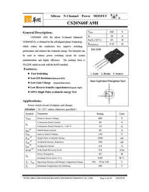
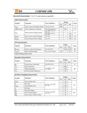
Silicon N-Channel Power MOSFET
R
○
CS20N60F A9H
VDSS 600 V
General Description:
ID 20 A
CS20N60F A9H, the silicon N-channel Enhanced
PD(TC=25℃) 85 W
VDMOSFETs, is obtained by the self-aligned planar Technology
RDS(ON)Typ 0.36 Ω
which reduce the conduction loss, improve switching
performance and enhance the avalanche energy. The transistor can
be used in various
3.6. cs20n60.pdf Size:109K _china
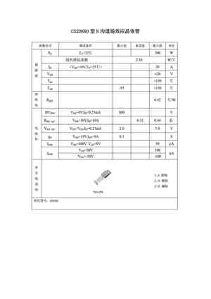
CS20N60 型 N 沟道场效应晶体管
参数符号 测试条件 最小值 典型值 最大值 单位
PD TC=25℃ 300 W
线性降低系数 2.38 W/℃
极
ID (VGS=10V,TC=25℃) 20 A
限
VGS ±20 V
值
Tjm +150 ℃
Tstg -55 +150 ℃
热
特
RthJC 0.42 ℃/W
性
BVDSS VGS=0V,ID=0.25mA 600 V
RDS on) VGS=10V,ID=10A 0.32 0.46 Ω
(
电
VGS th) VDS=VGS,ID=0.25m
3.7. cs20n60fa9h.pdf Size:2676K _citcorp
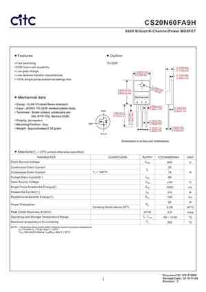
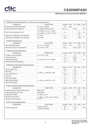
CS20N60FA9H
600V Silicon N-Channel Power MOSFET
■ Features ■ Outline
• Fast switching. TO-220F
• ESD improved capability.
0.189(4.80)
0.173(4.40)
• Low gate charge.
0.409(10.40)
0.378(9.60) 0.114(2.90)
• Low reverse transfer capacitances.
0.098(2.50)
• 100% single pulse avalanche energy test.
0.638(16.20)
0.606(15.40)
Marking code
■ Mechanical data
G D S
• Ep
SPW20N60C3 Datasheet (PDF)
1.1. spw20n60c3.pdf Size:765K _infineon
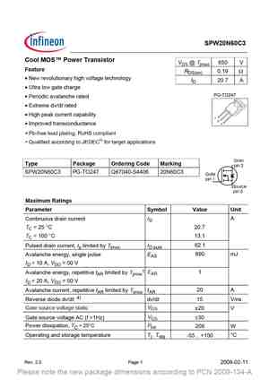
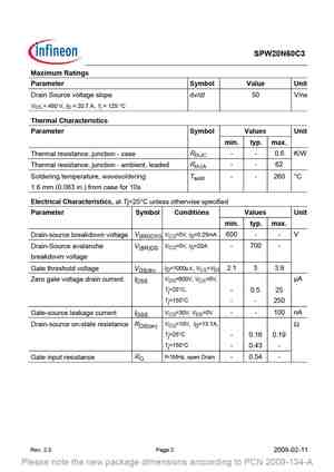
VDS Tjmax
Ω
•
•
G
•
•
•
•
G-TO247
1.2. spw20n60cfd.pdf Size:2950K _infineon
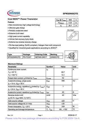

Please note the new package dimensions arccording to PCN 2009‐1 4‐A
Please note the new package dimensions arccording to PCN 2009‐1 4‐A
Please note the new package dimensions arccording to PCN 2009‐1 4‐A
Please note the new package dimensions arccording to PCN 2009‐1 4‐A
Please note the new package dimensions arccording to PCN 2009‐1 4‐A
Please note the new package
1.3. spw20n60c3.pdf Size:269K _inchange_semiconductor
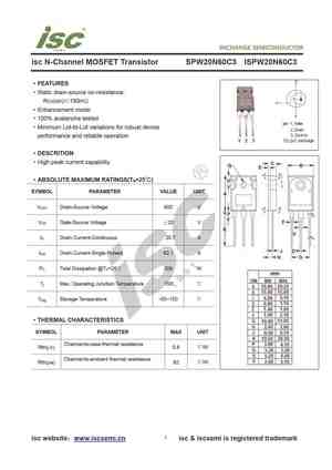
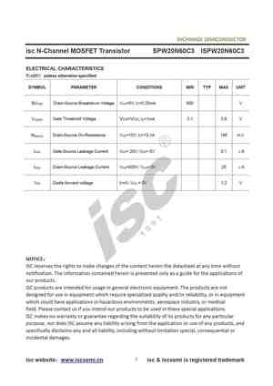
isc N-Channel MOSFET Transistor SPW20N60C3 ISPW20N60C3
·FEATURES
·Static drain-source on-resistance:
RDS(on)≤190mΩ
·Enhancement mode:
·100% avalanche tested
·Minimum Lot-to-Lot variations for robust device
performance and reliable operation
·DESCRITION
·High peak current capability
·ABSOLUTE MAXIMUM RATINGS(T =25℃)
a
SYMBOL PARAMETER VALUE UNIT
V Drain-Source Voltage
1.4. spw20n60cfd.pdf Size:245K _inchange_semiconductor
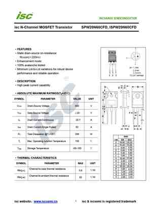
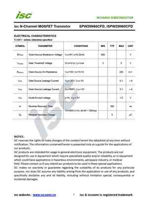
isc N-Channel MOSFET Transistor SPW20N60CFD, ISPW20N60CFD
·FEATURES
·Static drain-source on-resistance:
RDS(on)≤220mΩ
·Enhancement mode:
·100% avalanche tested
·Minimum Lot-to-Lot variations for robust device
performance and reliable operation
·DESCRIPTION
·High peak current capability
·ABSOLUTE MAXIMUM RATINGS(T =25℃)
a
SYMBOL PARAMETER VALUE UNIT
V Drain-Source Volt
SPW20N60S5 Datasheet (PDF)
1.1. spw20n60s5.pdf Size:768K _infineon
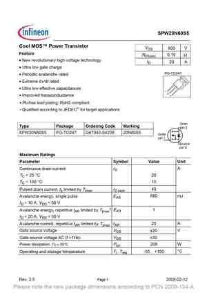
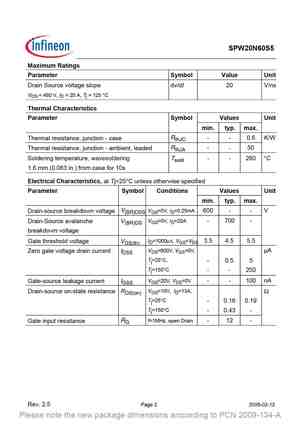
SPW20N60S5
Cool MOS Power Transistor
VDS
600 V
Feature
RDS(on) 0.19 Ω
• New revolutionary high voltage technology
ID 20 A
• Ultra low gate charge
PG-TO247
• Periodic avalanche rated
• Extreme dv/dt rated
• Ultra low effective capacitances
• Improved transconductance
Type Package Ordering Code Marking
SPW20N60S5 PG-TO247 Q67040-S4238 20N60S5
Maximum Ratings
Para
1.2. spw20n60s5.pdf Size:244K _inchange_semiconductor
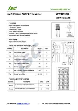

isc N-Channel MOSFET Transistor SPW20N60S5
ISPW20N60S5
·FEATURES
·Static drain-source on-resistance:
RDS(on)≤190mΩ
·Enhancement mode:
·100% avalanche tested
·Minimum Lot-to-Lot variations for robust device
performance and reliable operation
·DESCRITION
·Improved transconductance
·ABSOLUTE MAXIMUM RATINGS(T =25℃)
a
SYMBOL PARAMETER VALUE UNIT
V Drain-Source Voltage 60
2.1. spw20n60c3.pdf Size:765K _infineon


VDS Tjmax
Ω
•
•
G
•
•
•
•
G-TO247
2.2. spw20n60cfd.pdf Size:2950K _infineon


Please note the new package dimensions arccording to PCN 2009‐1 4‐A
Please note the new package dimensions arccording to PCN 2009‐1 4‐A
Please note the new package dimensions arccording to PCN 2009‐1 4‐A
Please note the new package dimensions arccording to PCN 2009‐1 4‐A
Please note the new package dimensions arccording to PCN 2009‐1 4‐A
Please note the new package
2.3. spw20n60c3.pdf Size:269K _inchange_semiconductor


isc N-Channel MOSFET Transistor SPW20N60C3 ISPW20N60C3
·FEATURES
·Static drain-source on-resistance:
RDS(on)≤190mΩ
·Enhancement mode:
·100% avalanche tested
·Minimum Lot-to-Lot variations for robust device
performance and reliable operation
·DESCRITION
·High peak current capability
·ABSOLUTE MAXIMUM RATINGS(T =25℃)
a
SYMBOL PARAMETER VALUE UNIT
V Drain-Source Voltage
2.4. spw20n60cfd.pdf Size:245K _inchange_semiconductor


isc N-Channel MOSFET Transistor SPW20N60CFD, ISPW20N60CFD
·FEATURES
·Static drain-source on-resistance:
RDS(on)≤220mΩ
·Enhancement mode:
·100% avalanche tested
·Minimum Lot-to-Lot variations for robust device
performance and reliable operation
·DESCRIPTION
·High peak current capability
·ABSOLUTE MAXIMUM RATINGS(T =25℃)
a
SYMBOL PARAMETER VALUE UNIT
V Drain-Source Volt
FCA20N60S Datasheet (PDF)
1.1. fca20n60s fca20n60s f109.pdf Size:750K _upd-mosfet
August 2007
TM
SuperFET
FCA20N60S / FCA20N60S_F109
600V N-Channel MOSFET
Features Description
• 650V @TJ = 150°C SuperFETTM is, Farichild’s proprietary, new generation of high
voltage MOSFET family that is utilizing an advanced charge
• Typ. Rds(on)=0.22Ω
balance mechanism for outstanding low on-resistance and
• Ultra low gate charge (typ. Qg=55nC) lower gate charge perform
1.2. fca20n60s fca20n60s f109.pdf Size:750K _fairchild_semi
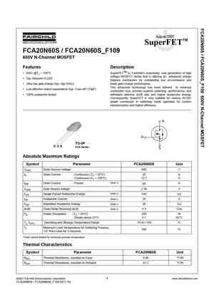
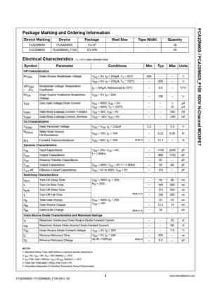
August 2007
TM
SuperFET
FCA20N60S / FCA20N60S_F109
600V N-Channel MOSFET
Features Description
• 650V @TJ = 150°C SuperFETTM is, Farichild’s proprietary, new generation of high
voltage MOSFET family that is utilizing an advanced charge
• Typ. Rds(on)=0.22Ω
balance mechanism for outstanding low on-resistance and
• Ultra low gate charge (typ. Qg=55nC) lower gate charge perform
2.1. fca20n60fs.pdf Size:952K _upd-mosfet
December 2008
TM
SuperFET
FCA20N60F
600V N-CHANNEL FRFET
Features Description
• 650V @TJ = 150°C SuperFETTM is, Fairchild’s proprietary, new generation of high
voltage MOSFET family that is utilizing an advanced charge
• Typ. Rds(on)=0.15Ω
balance mechanism for outstanding low on-resistance and
• Fast Recovery Type ( trr = 160ns ) lower gate charge performance.
This a
2.2. fch20n60 fca20n60 fca20n60 f109.pdf Size:971K _fairchild_semi
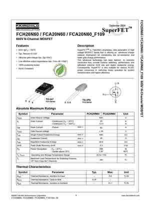

December 2008
TM
SuperFET
FCH20N60 / FCA20N60 / FCA20N60_F109
600V N-Channel MOSFET
Features Description
• 650V @TJ = 150°C SuperFETTM is, Fairchild’s proprietary, new generation of high
voltage MOSFET family that is utilizing an advanced charge
• Typ. Rds(on)=0.15Ω
balance mechanism for outstanding low on-resistance and
• Ultra low gate charge (typ. Qg=55nC) lower gate cha
2.3. fca20n60f fca20n60fs.pdf Size:952K _fairchild_semi
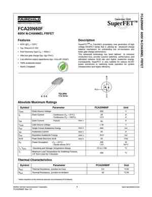
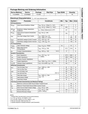
December 2008
TM
SuperFET
FCA20N60F
600V N-CHANNEL FRFET
Features Description
• 650V @TJ = 150°C SuperFETTM is, Fairchild’s proprietary, new generation of high
voltage MOSFET family that is utilizing an advanced charge
• Typ. Rds(on)=0.15Ω
balance mechanism for outstanding low on-resistance and
• Fast Recovery Type ( trr = 160ns ) lower gate charge performance.
This a
2.4. fca20n60 fca20n60 f109.pdf Size:481K _fairchild_semi
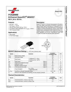
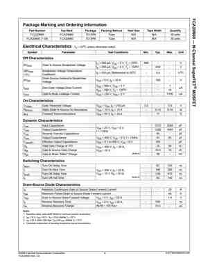
August 2014
FCA20N60
N-Channel SuperFET MOSFET
600 V, 20 A, 190 mΩ
Features Description
SuperFET MOSFET is Fairchild Semiconductor’s first genera-
• 650V @ TJ = 150°C
tion of high voltage super-junction (SJ) MOSFET family that is
• Typ. RDS(on) = 150 mΩ
utilizing charge balance technology for outstanding low on-
• Ultra Low Gate Charge (Typ. Qg = 75 nC )
resistance an
CS1N60_C3H Datasheet (PDF)
1.1. cs1n60 c3h.pdf Size:530K _crhj
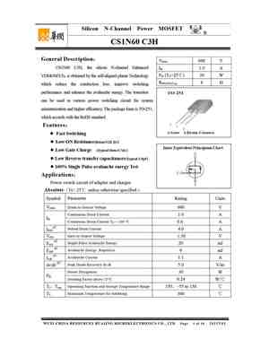
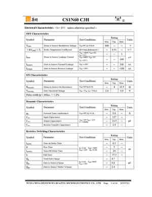
Silicon N-Channel Power MOSFET R
○
CS1N60 C3H
General Description:
VDSS 600 V
CS1N60 C3H, the silicon N-channel Enhanced
ID 1.0 A
PD (TC=25℃) 30 W
VDMOSFETs, is obtained by the self-aligned planar Technology
RDS(ON)Typ 8 Ω
which reduce the conduction loss, improve switching
performance and enhance the avalanche energy. The transistor
can be used in various power s
2.1. cs1n60 c1h.pdf Size:483K _crhj
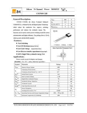

Silicon N-Channel Power MOSFET R
○
CS1N60 C1H
General Description:
VDSS 600 V
CS1N60 C1H-BD, the silicon N-channel Enhanced
ID 1.0 A
PD (TC=25℃) 3 W
VDMOSFETs, is obtained by the self-aligned planar Technology
RDS(ON)Typ 9 Ω
which reduce the conduction loss, improve switching
performance and enhance the avalanche energy. The
transistor can be used in various power
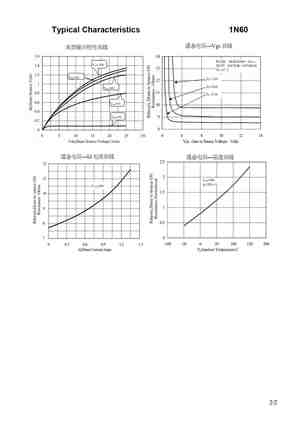
3.1. cs1n60 to-92.pdf Size:245K _can-sheng
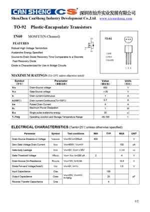
深圳市灿升实业发展有限公司
ShenZhen CanSheng Industry Development Co.,Ltd. www.szcansheng.com
TO-92 Plastic-Encapsulate Transistors
1N60 MOSFET(N-Channel)
FEATURES
Robust High Voltage Terminrtion
Avalanche Energy Specified
Source-to-Drain Diode Recovery Time Comparable to a Discrete
Fast Recovery Diode
Diode is Characterrized for Use in Bridge Circuits
MAXIMU
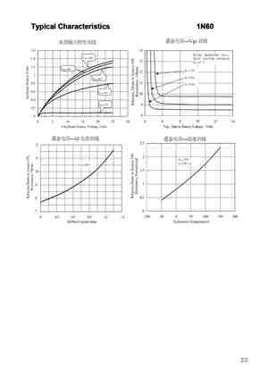
3.2. cs1n60 to-252.pdf Size:241K _can-sheng
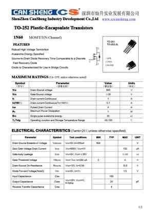
深圳市灿升实业发展有限公司
ShenZhen CanSheng Industry Development Co.,Ltd
ShenZhen CanSheng Industry Development Co.,Ltd
ShenZhen CanSheng Industry Development Co.,Ltd www.szcansheng.com
ShenZhen CanSheng Industry Development Co.,Ltd.
TO-252 Plastic-Encapsulate Transistors
TO-252 Plastic-Encapsulate Transistors
TO-252 Plastic-Encapsulate Transistors
TO-252 Plastic-Encapsula
3.3. cs1n60 a1h.pdf Size:537K _crhj
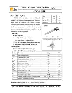
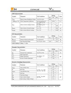
Silicon N-Channel Power MOSFET R
○
CS1N60 A1H
General Description:
VDSS 600 V
CS1N60 A1H, the silicon N-channel Enhanced
ID 0.8 A
PD (TC=25℃) 3 W
VDMOSFETs, is obtained by the self-aligned planar Technology
RDS(ON)Typ 11 Ω
which reduce the conduction loss, improve switching
performance and enhance the avalanche energy. The transistor
can be used in various power
3.4. cs1n60 a3h.pdf Size:532K _crhj
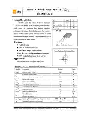

Silicon N-Channel Power MOSFET R
○
CS1N60 A3H
General Description:
VDSS 600 V
CS1N60 A3H, the silicon N-channel Enhanced
ID 0.8 A
PD (TC=25℃) 25 W
VDMOSFETs, is obtained by the self-aligned planar Technology
RDS(ON)Typ 11 Ω
which reduce the conduction loss, improve switching
performance and enhance the avalanche energy. The transistor
can be used in various power
3.5. cs1n60 b1r.pdf Size:1006K _crhj
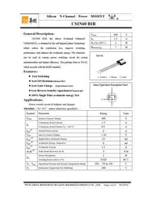
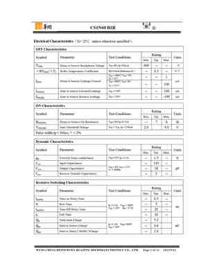
Silicon N-Channel Power MOSFET R
○
CS1N60 B1R
General Description:
VDSS 600 V
CS1N60 B1R, the silicon N-channel Enhanced
ID 1.5 A
PD (TC=25℃) 3 W
VDMOSFETs, is obtained by the self-aligned planar Technology
RDS(ON)Typ 7 Ω
which reduce the conduction loss, improve switching
performance and enhance the avalanche energy. The transistor
can be used in various power s
3.6. cs1n60 b3r.pdf Size:991K _crhj
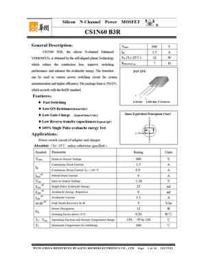

Silicon N-Channel Power MOSFET R
○
CS1N60 B3R
General Description:
VDSS 600 V
CS1N60 B3R, the silicon N-channel Enhanced
ID 1.5 A
PD (TC=25℃) 32 W
VDMOSFETs, is obtained by the self-aligned planar Technology
RDS(ON)Typ 7 Ω
which reduce the conduction loss, improve switching
performance and enhance the avalanche energy. The transistor
can be used in various power s
CS20N60_A8H MOSFET — описание производителя. Даташиты. Основные параметры и характеристики. Поиск аналога. Справочник
Наименование прибора: CS20N60_A8H
Тип транзистора: MOSFET
Полярность: N
Максимальная рассеиваемая мощность (Pd): 250
W
Предельно допустимое напряжение сток-исток (Uds): 600
V
Предельно допустимое напряжение затвор-исток (Ugs): 30
V
Максимально допустимый постоянный ток стока (Id): 20
A
Максимальная температура канала (Tj): 150
°C
Время нарастания (tr): 73
ns
Выходная емкость (Cd): 252
pf
Сопротивление сток-исток открытого транзистора (Rds): 0.45
Ohm
Тип корпуса: TO220AB
CS20N60_A8H
Datasheet (PDF)
1.1. cs20n60 anh.pdf Size:437K _crhj


Silicon N-Channel Power MOSFET R
○
CS20N60 ANH
VDSS 600 V
General Description:
ID 20 A
CS20N60 ANH, the silicon N-channel Enhanced
PD(TC=25℃) 250 W
VDMOSFETs, is obtained by the self-aligned planar Technology
RDS(ON)Typ 0.36 Ω
which reduce the conduction loss, improve switching
performance and enhance the avalanche energy. The transistor can
be used in various po
1.2. cs20n60 a8h.pdf Size:434K _crhj


Silicon N-Channel Power MOSFET R
○
CS20N60 A8H
VDSS 600 V
General Description:
ID 20 A
CS20N60 A8H, the silicon N-channel Enhanced
PD(TC=25℃) 250 W
VDMOSFETs, is obtained by the self-aligned planar Technology
RDS(ON)Typ 0.36 Ω
which reduce the conduction loss, improve switching
performance and enhance the avalanche energy. The transistor can
be used in various po
3.1. cs20n60a8h.pdf Size:434K _update_mosfet
Silicon N-Channel Power MOSFET R
○
CS20N60 A8H
VDSS 600 V
General Description:
ID 20 A
CS20N60 A8H, the silicon N-channel Enhanced
PD(TC=25℃) 250 W
VDMOSFETs, is obtained by the self-aligned planar Technology
RDS(ON)Typ 0.36 Ω
which reduce the conduction loss, improve switching
performance and enhance the avalanche energy. The transistor can
be used in various po
3.2. cs20n60.pdf Size:109K _update_mosfet
CS20N60 型 N 沟道场效应晶体管
参数符号 测试条件 最小值 典型值 最大值 单位
PD TC=25℃ 300 W
线性降低系数 2.38 W/℃
极
ID (VGS=10V,TC=25℃) 20 A
限
VGS ±20 V
值
Tjm +150 ℃
Tstg -55 +150 ℃
热
特
RthJC 0.42 ℃/W
性
BVDSS VGS=0V,ID=0.25mA 600 V
RDS on) VGS=10V,ID=10A 0.32 0.46 Ω
(
电
VGS th) VDS=VGS,ID=0.25m
3.3. cs20n60anh.pdf Size:437K _update_mosfet
Silicon N-Channel Power MOSFET R
○
CS20N60 ANH
VDSS 600 V
General Description:
ID 20 A
CS20N60 ANH, the silicon N-channel Enhanced
PD(TC=25℃) 250 W
VDMOSFETs, is obtained by the self-aligned planar Technology
RDS(ON)Typ 0.36 Ω
which reduce the conduction loss, improve switching
performance and enhance the avalanche energy. The transistor can
be used in various po
3.4. cs20n60fa9h.pdf Size:2676K _update_mosfet
CS20N60FA9H
600V Silicon N-Channel Power MOSFET
■ Features ■ Outline
• Fast switching. TO-220F
• ESD improved capability.
0.189(4.80)
0.173(4.40)
• Low gate charge.
0.409(10.40)
0.378(9.60) 0.114(2.90)
• Low reverse transfer capacitances.
0.098(2.50)
• 100% single pulse avalanche energy test.
0.638(16.20)
0.606(15.40)
Marking code
■ Mechanical data
G D S
• Ep
3.5. cs20n60f a9h.pdf Size:431K _crhj


Silicon N-Channel Power MOSFET
R
○
CS20N60F A9H
VDSS 600 V
General Description:
ID 20 A
CS20N60F A9H, the silicon N-channel Enhanced
PD(TC=25℃) 85 W
VDMOSFETs, is obtained by the self-aligned planar Technology
RDS(ON)Typ 0.36 Ω
which reduce the conduction loss, improve switching
performance and enhance the avalanche energy. The transistor can
be used in various
3.6. cs20n60.pdf Size:109K _china

CS20N60 型 N 沟道场效应晶体管
参数符号 测试条件 最小值 典型值 最大值 单位
PD TC=25℃ 300 W
线性降低系数 2.38 W/℃
极
ID (VGS=10V,TC=25℃) 20 A
限
VGS ±20 V
值
Tjm +150 ℃
Tstg -55 +150 ℃
热
特
RthJC 0.42 ℃/W
性
BVDSS VGS=0V,ID=0.25mA 600 V
RDS on) VGS=10V,ID=10A 0.32 0.46 Ω
(
电
VGS th) VDS=VGS,ID=0.25m
3.7. cs20n60fa9h.pdf Size:2676K _citcorp


CS20N60FA9H
600V Silicon N-Channel Power MOSFET
■ Features ■ Outline
• Fast switching. TO-220F
• ESD improved capability.
0.189(4.80)
0.173(4.40)
• Low gate charge.
0.409(10.40)
0.378(9.60) 0.114(2.90)
• Low reverse transfer capacitances.
0.098(2.50)
• 100% single pulse avalanche energy test.
0.638(16.20)
0.606(15.40)
Marking code
■ Mechanical data
G D S
• Ep
Другие MOSFET… SID40N03
, SID9435
, SID9575
, SID9971
, SJV01N60
, SMG1330N
, SMG2301
, SMG2301P
, IRF540N
, SMG2302N
, SMG2305
, SMG2305P
, SMG2305PE
, SMG2306A
, SMG2306N
, SMG2306NE
, SMG2310A
.
SPI20N60CFD Datasheet (PDF)
1.1. spp20n60c3 spi20n60c3 spa20n60c3 rev3.2.pdf Size:683K _infineon


SPP20N60C3
SPI20N60C3, SPA20N60C3
Cool MOS Power Transistor
VDS @ Tjmax 650 V
Feature
RDS(on) 0.19 Ω
• New revolutionary high voltage technology
ID 20.7 A
• Worldwide best RDS(on) in TO 220
PG-TO220FP PG-TO262 PG-TO220
• Ultra low gate charge
• Periodic avalanche rated
3
• Extreme dv/dt rated
2
1
P-TO220-3-31
• High peak current capability
• Improved transco
1.2. spi20n60cfd.pdf Size:554K _infineon
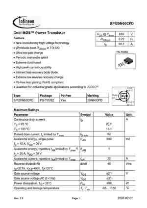
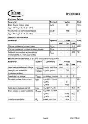
SPI20N60CFD
CססI MOS Pסwer Transistסr
VDS @ Tjmax 650 V
Feature
RDS(on) 0.22
• New revolutionary high voltage technology
ID 20.7 A
• Worldwide best RDS(on) in TO 220
PG-TO262
• Ultra low gate charge
• Periodic avalanche rated
• Extreme dv/dt rated
• High peak current capability
• Intrinsic fast-recovery body diode
• Extreme low reverse recovery charge
Qualifi
1.3. spp20n60c3 spi20n60c3 spa20n60c3.pdf Size:1832K _infineon


SPP20N60C3
SPI20N60C3, SPA20N60C3
Cool MOS Power Transistor
VDS @ Tjmax 650 V
Feature
RDS(on) 0.19 Ω
• New revolutionary high voltage technology
ID 20.7 A
• Worldwide best RDS(on) in TO 220
PG-TO220FP PG-TO262 PG-TO220
• Ultra low gate charge
• Periodic avalanche rated
3
• Extreme dv/dt rated
2
1
P-TO220-3-31
• High peak current capability
• Improved transco
1.4. spi20n60c3.pdf Size:215K _inchange_semiconductor
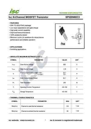
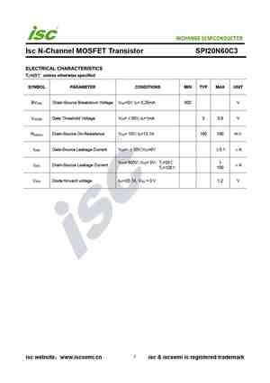
INCHANGE Semiconductor
Isc N-Channel MOSFET Transistor SPI20N60C3
·FEATURES
·With TO-262(I2PAK) package
·Low input capacitance and gate charge
·High peak current capability
·Improved transconductance
·100% avalanche tested
·Minimum Lot-to-Lot variations for robust device
performance and reliable operation
·APPLICATIONS
·Switching applications
·ABSOLUTE MAXIMUM RATINGS(T =2
